
Semiconductor device and manufacturing method thereof

A semiconductor and device technology, applied in the field of semiconductor devices and their production, can solve problems such as increasing device thermal power consumption, affecting device performance, increasing device junction temperature, etc., to reduce complexity, improve static electricity resistance, and improve reliability Effect

Active Publication Date: 2021-08-31
GPOWER SEMICON
View PDF4 Cites 0 Cited by
  • Summary
  • Abstract
  • Description
  • Claims
  • Application Information

AI Technical Summary

Problems solved by technology

Since the energy loss of avalanche breakdown and device turn-on is proportional to the operating frequency and the amount of mismatched charges, the high-voltage depletion-mode AlGaN / GaN semiconductor device in the enhancement mode cascode semiconductor device. Capacitance and capacitance mismatch between the source and drain of low-voltage enhancement-mode Si-MOSFET directly affect the high-frequency application of this enhancement-mode cascode semiconductor device, and the additional energy loss also increases the thermal power consumption of the device, Increase the junction temperature of the device and affect the performance of the device

Method used


Image

  • Semiconductor device and manufacturing method thereof
  • Semiconductor device and manufacturing method thereof
  • Semiconductor device and manufacturing method thereof

Examples


Embodiment Construction

[0046] The following will clearly and completely describe the technical solutions in the embodiments of the present invention with reference to the accompanying drawings in the embodiments of the present invention. Obviously, the described embodiments are only some, not all, embodiments of the present invention. The components of the embodiments of the invention generally described and illustrated in the figures herein may be arranged and designed in a variety of different configurations. Accordingly, the following detailed description of the embodiments of the invention provided in the accompanying drawings is not intended to limit the scope of the claimed invention, but merely represents selected embodiments of the invention. Based on the embodiments of the present invention, all other embodiments obtained by those skilled in the art without making creative efforts belong to the protection scope of the present invention.

[0047]It should be noted that like numerals and lett...


PUM


Abstract

The invention provides a semiconductor device and a manufacturing method thereof, which relate to the technical field of semiconductors. By introducing a second dielectric layer with a higher dielectric constant between the two plates constituting the gate-source capacitance, the gate-source capacitance of the semiconductor device is increased, and the drain-source capacitance of the semiconductor device and the connection with the semiconductor device are solved. The problem of mutual mismatch between the drain-source capacitances of other semiconductor devices in cascaded devices does not require an external capacitor connected in parallel between the source and drain of the semiconductor device, which can reduce the complexity of the circuit and the volume of the semiconductor device, and can improve the performance of the semiconductor device. The reliability of the device can improve the electrostatic resistance of the device by introducing a high dielectric constant material between the two field plates that form the gate-source capacitance.

Description

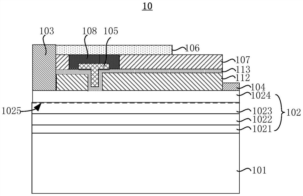
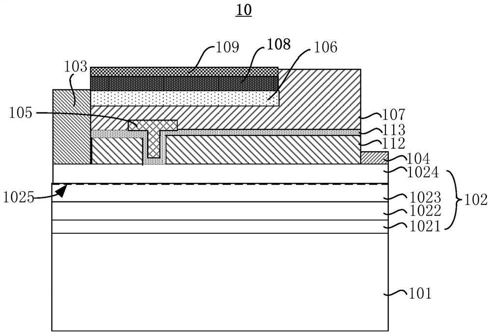
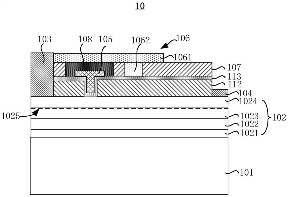
technical field [0001] The present invention relates to the technical field of semiconductors, in particular to a semiconductor device and a manufacturing method thereof. Background technique [0002] GaN (gallium nitride) semiconductor devices have significant advantages such as large band gap, high electron mobility, high breakdown field strength, and high temperature resistance. Compared with the first-generation semiconductor silicon and the second-generation semiconductor gallium arsenide, it is more suitable It has broad application prospects for making high-temperature, high-voltage, high-frequency and high-power electronic devices. [0003] In radio frequency microwave and high-voltage applications, enhanced semiconductor devices are essential, and high-voltage depletion-type AlGaN / GaN semiconductor devices and low-voltage enhanced silicon-metal-oxide-semiconductor field-effect transistors (Si-Metal-Oxide-Semiconductor Field) are often used -Effect Transistor, Si-MO...

Claims


Application Information

Patent Timeline
Patent Type & Authority Patents(China)
IPC IPC(8): H01L29/778H01L21/335H01L29/40
CPCH01L29/402H01L29/66462H01L29/778
Inventor 吴俊峰邓光敏吴星星
Owner GPOWER SEMICON
Learn More