Semiconductor device and preparation method thereof

A semiconductor and device technology, applied in the field of semiconductor devices and their production, can solve problems such as capacitance mismatch, achieve the effect of increasing gate-source capacitance and solving mutual mismatch

Active Publication Date: 2016-02-10
GPOWER SEMICON
View PDF3 Cites 11 Cited by
  • Summary
  • Abstract
  • Description
  • Claims
  • Application Information

AI Technical Summary

Problems solved by technology

[0005] The purpose of the present invention is to propose a semiconductor device and a manufacturing method thereof, which can solve the problem of the capacitance between the source and the drain of the high-voltage depletion-type AlGaN / GaN semiconductor device in the prior art. Capacitance Mismatch between Source and Drain of Low Voltage Enhancement Mode Si-MOSFET

Method used


Image

  • Semiconductor device and preparation method thereof
  • Semiconductor device and preparation method thereof
  • Semiconductor device and preparation method thereof

Examples


Embodiment 1

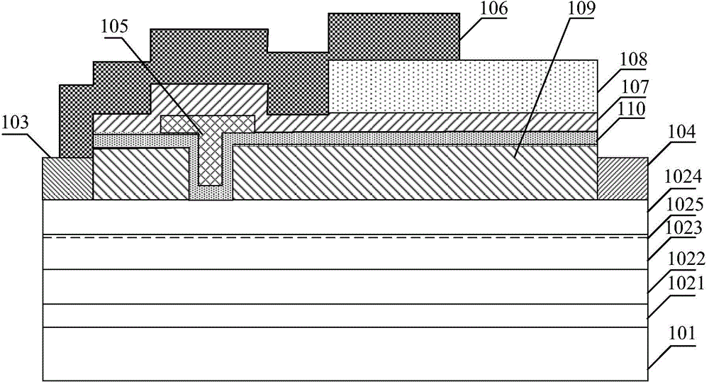
[0044] figure 1 is a schematic cross-sectional view of the semiconductor device provided by Embodiment 1 of the present invention. Such as figure 1 As shown, the semiconductor device includes:

[0045] Substrate 101.

[0046] In this embodiment, the material of the substrate 101 can be sapphire, silicon nitride, gallium nitride, silicon or other materials suitable for growing gallium nitride; the deposition method of the substrate 101 can be atmospheric pressure chemical vapor deposition (APCVD) , Subatmospheric pressure chemical vapor deposition (SACVD), metal organic compound chemical vapor deposition (MOCVD), low pressure chemical vapor deposition (LPCVD), high density plasma chemical vapor deposition (HDCVD), ultra-high vacuum chemical vapor deposition Deposition method (UHCVD), plasma enhanced chemical vapor deposition method (PlasmaEnhancedChemicalVaporDeposition, referred to as PECVD), catalytic chemical vapor deposition method (Cat-CVD), mixture physical and chemica...

Embodiment 2

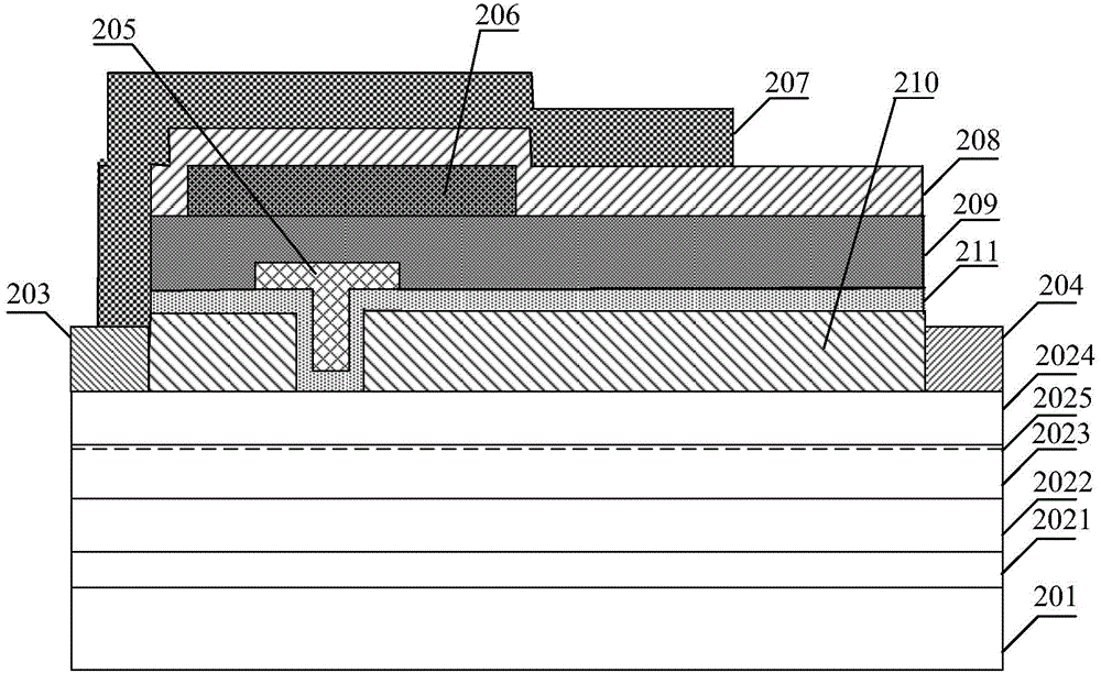
[0084] figure 2 is a schematic cross-sectional view of the semiconductor device provided by Embodiment 2 of the present invention. Such as figure 2 As shown, the semiconductor device provided in the second embodiment includes:

[0085] Substrate 201.

[0086] In this embodiment, the material of the substrate 201 can be sapphire, silicon nitride, gallium nitride, silicon or other materials suitable for growing gallium nitride; the deposition method of the substrate 201 can be atmospheric pressure chemical vapor deposition (APCVD) , Subatmospheric pressure chemical vapor deposition (SACVD), metal organic compound chemical vapor deposition (MOCVD), low pressure chemical vapor deposition (LPCVD), high density plasma chemical vapor deposition (HDCVD), ultra-high vacuum chemical vapor deposition Deposition method (UHCVD), plasma enhanced chemical vapor deposition method (PlasmaEnhancedChemicalVaporDeposition, referred to as PECVD), catalytic chemical vapor deposition method (Ca...

Embodiment 3

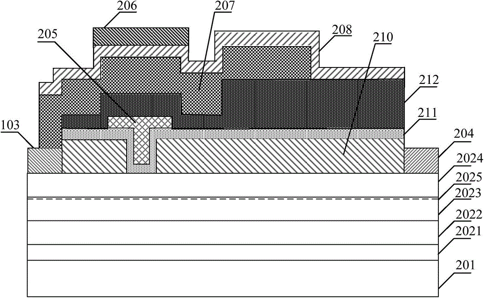
[0119] image 3 is a schematic cross-sectional view of the semiconductor device provided by Embodiment 3 of the present invention. Such as image 3 As shown, the difference from the semiconductor device provided in Embodiment 2 is that the gate field plate 206 of the semiconductor device provided in Embodiment 3 is located above the source field plate 207, and the semiconductor device does not include a second dielectric layer, But also include:

[0120] The third dielectric layer 212 is located between the gate 205 and the source field plate 207 .

[0121] In this embodiment, the third dielectric layer 212 is used to isolate the gate 205 and the source field plate 207; the smaller the thickness of the third dielectric layer 212, the larger the gate-source capacitance of the resulting semiconductor device.

[0122] Wherein, the material of the third dielectric layer 212 may be silicon nitride, silicon oxide, aluminum oxide or hafnium oxide; the manufacturing process of the ...


PUM


Abstract

The invention discloses a semiconductor device and a preparation method thereof. The semiconductor device comprises a substrate, a semiconductor layer, a source, a drain, a grid, a source field plate and a high dielectric constant dielectric layer, wherein the semiconductor layer is located on the substrate; the source and the drain are located on the semiconductor layer; the grid on the semiconductor layer is arranged between the source and the drain; the source field plate is electrically connected with the source; the high dielectric constant dielectric layer is located between the grid and the source field plate; and the dielectric constant of the high dielectric constant dielectric layer is greater than 3.9. The semiconductor device disclosed by the invention has relatively high gate-source capacitance, so that node capacitance of the semiconductor device and a structure cascaded with the semiconductor device can be matched with each other.

Description

technical field [0001] The invention relates to the technical field of semiconductors, in particular to a semiconductor device and a manufacturing method thereof. Background technique [0002] GaN (gallium nitride) semiconductor devices have significant advantages such as large band gap, high electron mobility, high breakdown field strength, and high temperature resistance. Compared with the first-generation semiconductor silicon and the second-generation semiconductor gallium arsenide, it is more suitable It has broad application prospects for making high-temperature, high-voltage, high-frequency and high-power electronic devices. [0003] Usually, AlGaN / GaN (aluminum gallium nitride / gallium nitride) semiconductor devices are depletion-mode devices. Due to the uniqueness of AlGaN and GaN materials, there are a large number of spontaneous polarization and The charge generated by piezoelectric polarization also has a high concentration of two-dimensional electron gas (Two-Di...

Claims


Application Information

Patent Timeline
Patent Type & Authority Applications(China)
IPC IPC(8): H01L29/778H01L29/06H01L29/40H01L21/335H01L21/28
CPCH01L29/0649H01L29/402H01L29/66462H01L29/778
Inventor 陈洪维裴轶张乃千
Owner GPOWER SEMICON
Why Eureka
Try Eureka