

How to deal with the burr in the pth connecting hole
A processing method and hole-connecting technology, applied in the processing of insulating substrates/layers, printed circuits, electrical components, etc., can solve problems such as poor draping effect, achieve simple operation, improve work efficiency, and reduce the number of stacked boards Effect
- Summary
- Abstract
- Description
- Claims
- Application Information
AI Technical Summary
Problems solved by technology
Method used
Image

Examples
Embodiment Construction
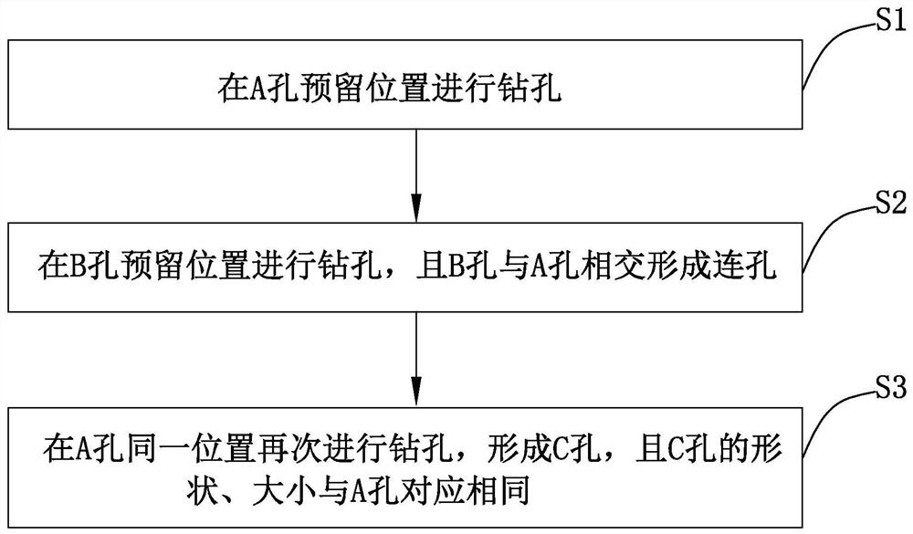
[0022] In order to enable those skilled in the art to better understand the technical solutions in the embodiments of the present invention, and to make the above-mentioned objects, features and advantages of the present invention more obvious and understandable, the specific implementation manners of the present invention will be further described below.
[0023] It should be noted here that the descriptions of these embodiments are used to help understand the present invention, but are not intended to limit the present invention. In addition, the technical features involved in the various embodiments of the present invention described below may be combined with each other as long as they do not conflict with each other.
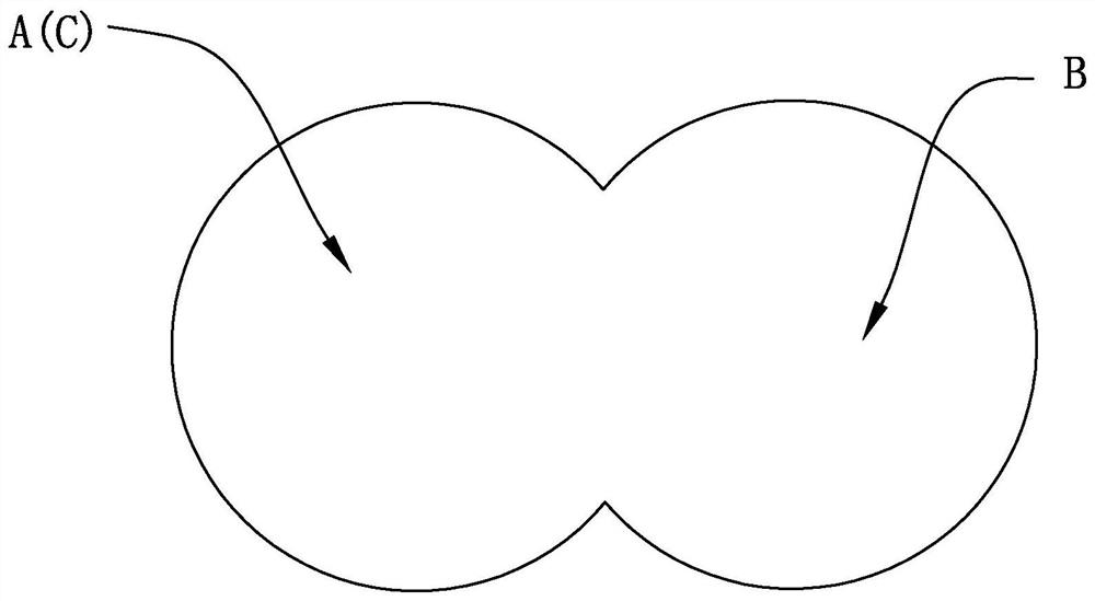
[0024] Please refer to figure 1 and figure 2 ,in figure 1 The flow chart of the processing method of the PTH connecting hole burr provided by the present invention; figure 2 It is a schematic diagram of the connected hole structure after the treatment ...
PUM
 Abstract
Description
Claims
Application Information