Film deposition method

A thin film deposition and process chamber technology, applied in ion implantation plating, metal material coating process, coating, etc., can solve the problems of product forward voltage increase, luminous intensity value decrease, and damage to the wafer surface. Achieve the effect of avoiding excessive energy and satisfying the sputtering rate

Active Publication Date: 2018-11-13
BEIJING NAURA MICROELECTRONICS EQUIP CO LTD
View PDF8 Cites 4 Cited by
  • Summary
  • Abstract
  • Description
  • Claims
  • Application Information

AI Technical Summary

Problems solved by technology

[0009] When the base 3 is in the figure 1 When the deposition process is performed at the process position shown, if RF power and DC power are applied to the target 2 at the same time, target particles with relatively high energy will be generated, which may damage the wafer surface when they are sputtered onto the wafer 4. It will cause the forward voltage value of the product to increase and the luminous intensity value to decrease, thus affecting product performance

Method used


Image

  • Film deposition method
  • Film deposition method
  • Film deposition method

Examples


Embodiment Construction

[0050] In order to enable those skilled in the art to better understand the technical solution of the present invention, the thin film deposition method provided by the present invention will be described in detail below with reference to the accompanying drawings.

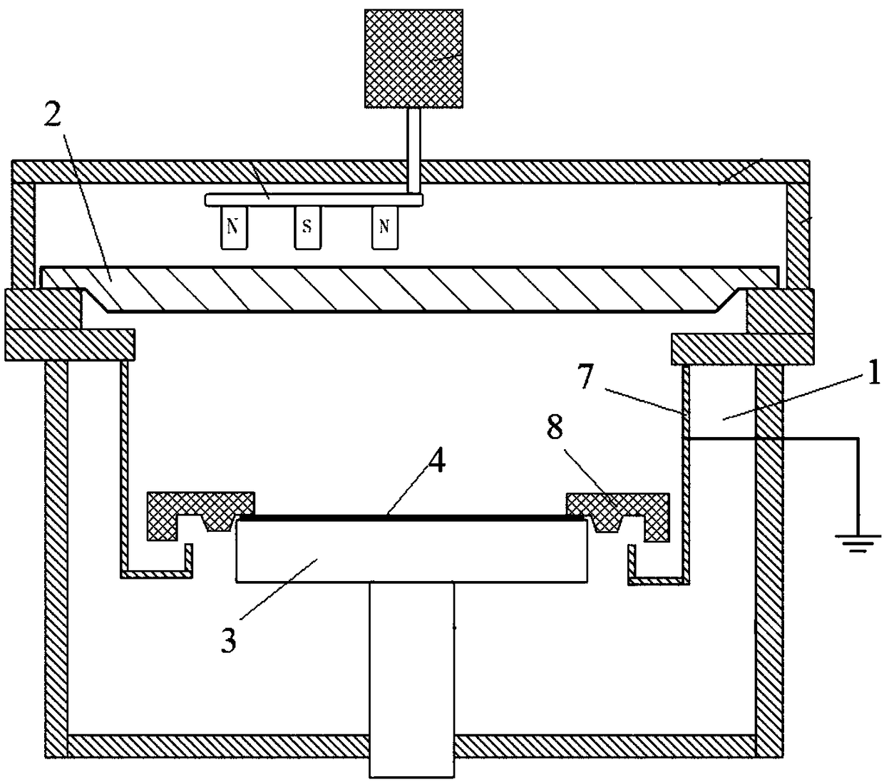
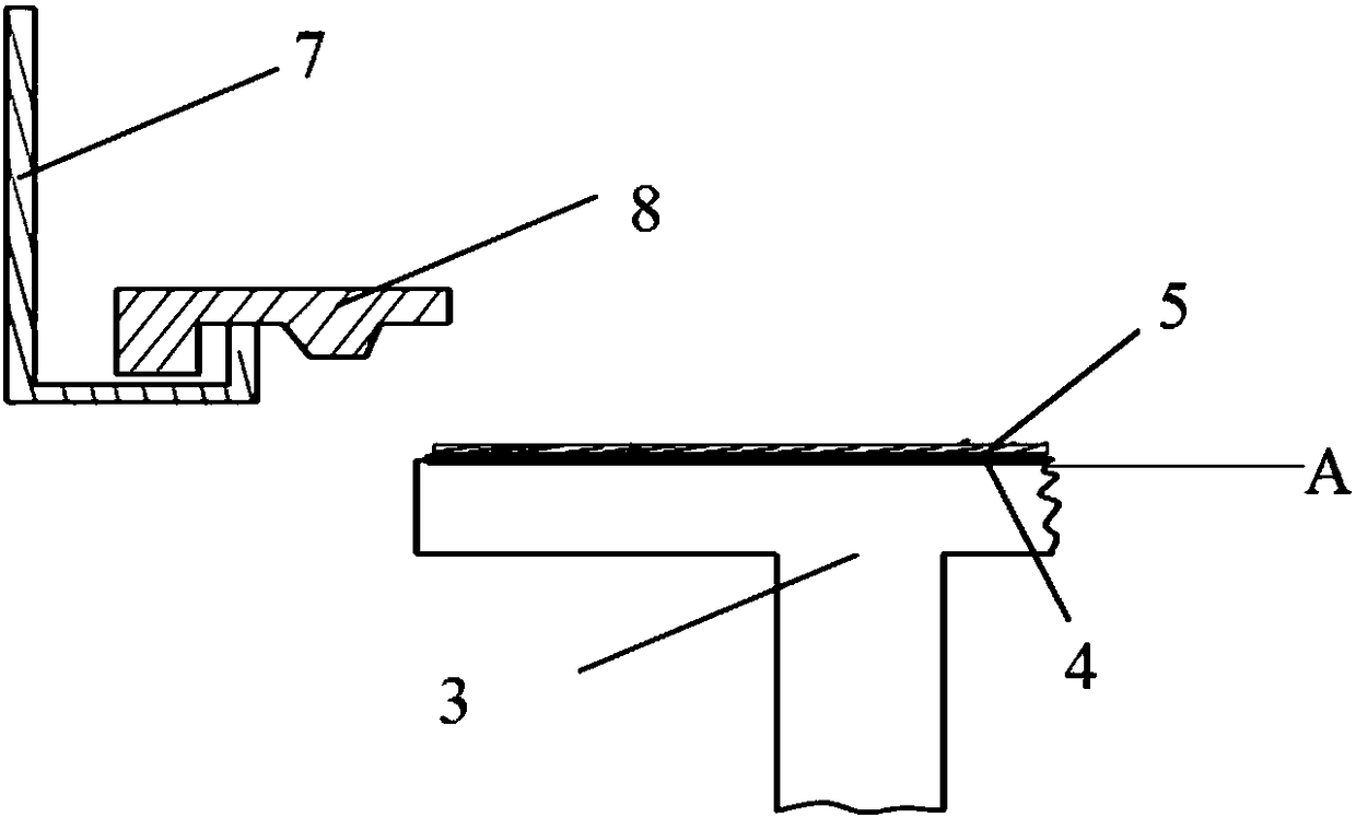
[0051] The process equipment used in the thin film deposition method provided by the embodiment of the present invention is as follows: figure 1 As shown, a process chamber 1 is included, and a target 2 is arranged on the top of the process chamber 1, and the target 2 is electrically connected to a radio frequency power supply and a DC power supply (both are not shown), that is, the target material 2 has Two access points, both of which are respectively connected to a radio frequency power supply and a DC power supply, are provided with a base 3 for carrying a wafer 4 in the process chamber 1 and below the target material 2 .

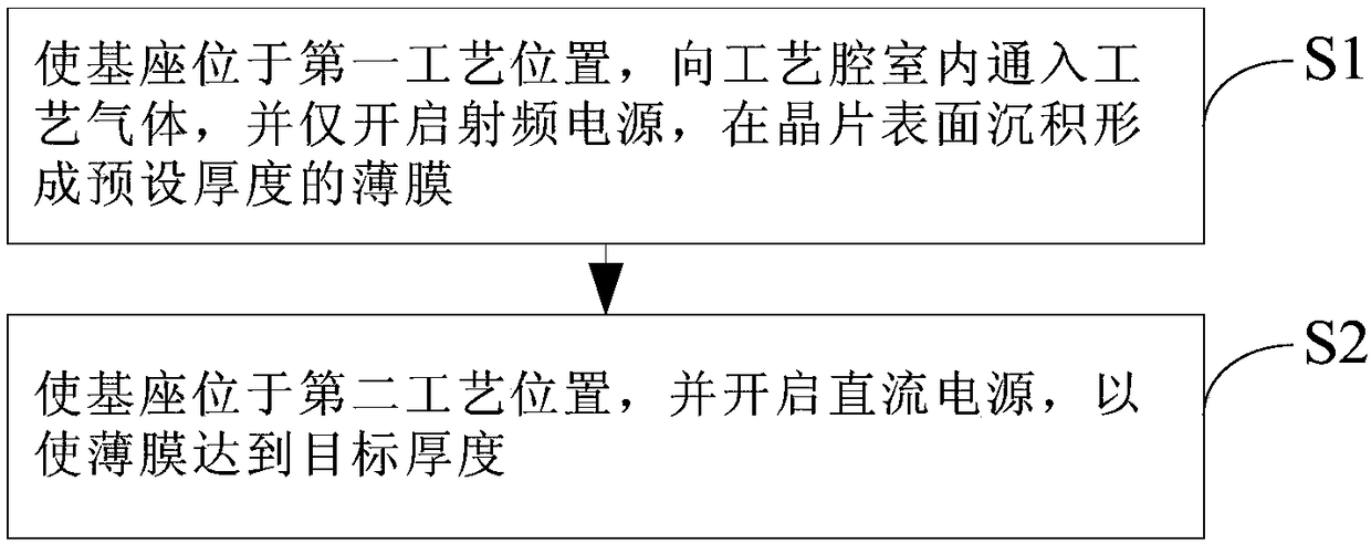
[0052] figure 2 The flow chart of the thin film deposition method provided by the emb...


PUM

PropertyMeasurementUnit
thicknessaaaaaaaaaa
thicknessaaaaaaaaaa

Abstract

The invention provides a film deposition method. The film deposition method comprises a first stage, specifically, in the first stage, a base is located at a first process position, a process gas is introduced into a process cavity, and only a radio-frequency power supply is started, so that a film with a preset thickness is deposited on the surface of a wafer; and a second stage, specifically, inthe second stage, the base is located at a second process position, a direct-current power supply is started, so that the thickness of the film is made to reach a target thickness, wherein the firstprocess position is lower than the second process position. According to the film deposition method, only radio-frequency power is loaded in the first stage so that the situation that the surface of the wafer is damaged due to the fact that the energy of generated target particles is too large can be avoided; and meanwhile, the first process position is lower than the second process position, so that it is ensured that the sputtering rate meets the process requirements under the condition that only the radio-frequency power is loaded.

Description

technical field [0001] The invention relates to the technical field of semiconductor manufacturing, in particular to a thin film deposition method. Background technique [0002] In the manufacturing process of LED chips, ITO film, as a transparent conductive film, has the advantages of high visible light transmittance, good conductivity, wear resistance and corrosion resistance compared with traditional metal films, and is widely used in GaN-based chips. electrode material. The preparation method of the ITO thin film includes the magnetron sputtering method, and the ITO thin film prepared by it has low resistivity, high visible light transmittance and high repeatability. [0003] figure 1 For the structure diagram of existing magnetron sputtering equipment, please refer to figure 1 , the magnetron sputtering equipment includes a process chamber 1, a target 2 is arranged on the top of the process chamber 1, the target 2 is electrically connected with a radio frequency powe...

Claims


Application Information

Patent Timeline
Patent Type & Authority Applications(China)
IPC IPC(8): C23C14/35
CPCC23C14/3492C23C14/35
Inventor 张同文耿波高攀罗建恒武学伟王厚工
Owner BEIJING NAURA MICROELECTRONICS EQUIP CO LTD
Why Eureka
Try Eureka