Check patentability & draft patents in minutes with Patsnap Eureka AI!

Detection method of scanning probe microscope with magnetic-electric signal detection function

A technology of scanning probe and detection method, which is applied in the field of scanning probe microscope, can solve the problems of high detection cost, affecting measurement accuracy, cumbersome scanning, etc., and achieve the effects of reducing detection cost, improving detection accuracy and simplifying the detection process

Active Publication Date: 2018-11-13
NINGBO INST OF MATERIALS TECH & ENG CHINESE ACADEMY OF SCI
View PDF6 Cites 8 Cited by
  • Summary
  • Abstract
  • Description
  • Claims
  • Application Information

AI Technical Summary

Problems solved by technology

Although this detection method is simple, there is a problem of too many scan times for the measurement of the magnetic properties and electrical properties of materials in the same micro-nano scale range. The electrical properties of the sample also require directional scanning. On the one hand, the scanning is cumbersome and the detection cost is high. On the other hand, it is difficult to suppress the sample drift under the condition of multiple scanning, which affects the measurement accuracy.

Method used


Image

  • Detection method of scanning probe microscope with magnetic-electric signal detection function

Examples


Embodiment 1

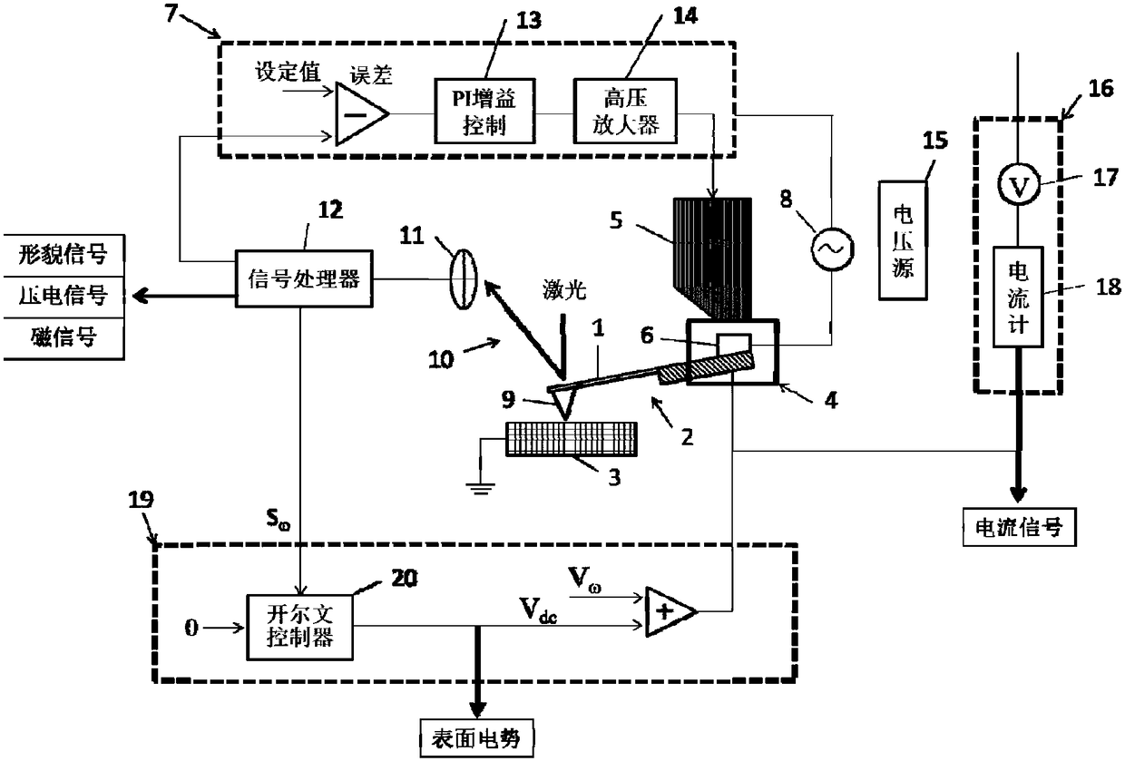
[0048] In this embodiment, the structure of the scanning probe microscope is as figure 1 As shown, the probe selects a commercial MESP probe with both conductivity and magnetism, and the SrTiO 3 CoFe grown on substrate 2 o 4 Magnetic films were used as samples. The sample was fixed on the scanning probe microscope platform, and the CoFe 2 o 4 The process of characterizing the morphology, conductivity and magnetic domains of the film is as follows:

[0049] (1) Under the action of the scanner 5, the probe scans the sample surface directionally from the initial position, and the contact mode is used during the scanning process, that is, the point contact between the probe tip and the sample surface is controlled

[0050] In the scanning process, the detection process at a certain scanning point is the following A process:

[0051] The change of the bending state of the probe cantilever 1 enters the photodetector 11 through the optical lever system 10 to be detected, and is...

Embodiment 2

[0059] In this embodiment, the structure of the scanning probe microscope is as figure 1 As shown, the probe selects a commercial MESP probe with both conductivity and magnetism, and the SrTiO 3 Growth of BiFeO with self-assembly characteristics on the substrate 3 -CoFe 2 o 4 film as a sample. Fix the sample on the scanning probe microscope platform, and use the scanning probe microscope to analyze the morphology of the film, BiFeO 3 Piezoelectric and CoFe 2 o 4 The process of characterizing the magnetic domains is as follows:

[0060] (1) Under the action of the scanner 5, the probe scans the sample surface directionally from the initial position, and the contact mode is used during the scanning process, that is, the point contact between the probe tip and the sample surface is controlled

[0061] In the scanning process, the detection process at a certain scanning point is the following A process:

[0062] The change of the bending state of the probe cantilever 1 ent...


PUM


Abstract

The invention provides a detection method of a scanning probe microscope with a magnetic-electric signal detection function; the method comprises the following steps: using a contact mode to simultaneously obtain a sample morphology signal and a conductive signal or morphology and piezoelectric signals in one scanning process, carrying out secondary scanning, and using a non-contact mode to obtaina sample magnetic signal. Compared with the prior art, the detection method simplifies a detection process, can effectively realize sample electricity characteristics that include a conductive characteristic and a piezoelectric characteristic and magnetic symptoms, can reduce a detection cost, and can improve the detection precision. In addition, the method preferably imports a Kelvin controllerin the scanning probe microscope system so as to eliminate electrostatic force, thus effectively preventing sample surface electromotive force interference in magnetic signal measurements, and improving test accuracy.

Description

technical field [0001] The invention relates to a scanning probe microscope with the function of measuring magneto-electric signals. Background technique [0002] The explosive growth of the current information volume puts forward higher requirements on the memory. As one of the most potential memories, magnetoelectric random access memory has advantages in terms of stability and low power consumption. In magnetoelectric random access memory, how to effectively use ferroelectric materials to effectively control the magnetic moment of the ferromagnetic layer is one of the important contents of its research. To this end, it is necessary to find a means to effectively characterize the magnetic and electrical properties, including conductivity and piezoelectricity. [0003] Scanning probe microscopy (SPM) uses the interaction force between the sample and the nanoprobe to detect the basic physical properties of the sample (such as morphology, magnetism, piezoelectricity, etc.),...

Claims


Application Information

Patent Timeline
IPC IPC(8): G01Q10/00G01Q60/52G01Q60/54G01Q30/18G01Q30/20G05B11/42
CPCG01Q10/00G01Q30/18G01Q30/20G01Q60/52G01Q60/54G05B11/42
Inventor 杨华礼王保敏李润伟郭姗姗陈斌
Owner NINGBO INST OF MATERIALS TECH & ENG CHINESE ACADEMY OF SCI
Features
  • R&D
  • Intellectual Property
  • Life Sciences
  • Materials
  • Tech Scout
  • Unparalleled Data Quality
  • Higher Quality Content
  • 60% Fewer Hallucinations
Learn More