Alkaline stripping solution for photoresists

A technology of photoresist and stripping solution, which is applied in the field of microelectronics, can solve the problems of rear Ti/Ni/Ag oxidation, white spots, and chromatic aberration, and achieve the effect of preventing white spots and chromatic aberration

Inactive Publication Date: 2018-11-13
KUNSHAN SIGO MICROELECTRONICS MATERIALS
View PDF3 Cites 4 Cited by
  • Summary
  • Abstract
  • Description
  • Claims
  • Application Information

AI Technical Summary

Problems solved by technology

The current annealing process is very easy to cause the back Ti / Ni / Ag to be oxidized, resulting in white spots and chromatic aberration
At present, there is no photoresist stripping solution in the market that can completely solve the white spot and color difference after stripping and high temperature annealing

Method used


Image

  • Alkaline stripping solution for photoresists
  • Alkaline stripping solution for photoresists
  • Alkaline stripping solution for photoresists

Examples


Embodiment Construction

[0026] The advantages of the present invention are further described below through specific examples, but the protection scope of the present invention is not limited only to the following examples.

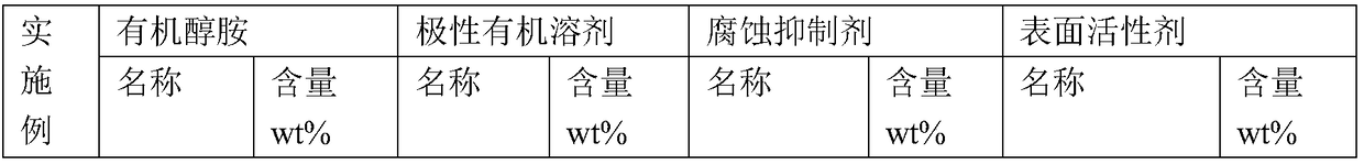
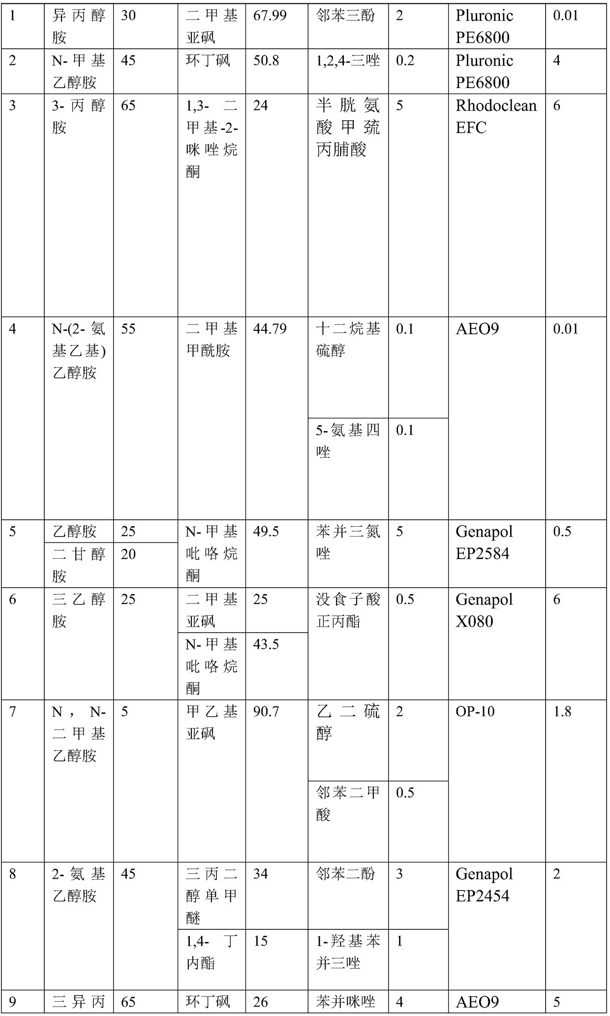
[0027] Component and content of table 1 embodiment and comparative example cleaning solution:

[0028] Table 1

[0029]

[0030]

[0031]

[0032] In order to further investigate the implementation effect of the photoresist stripping solution, the present invention adopts the following technical means: the 6-inch power semiconductor wafer chip whose back gold is Ti / Ni / Ag is cut into coupon wafers of 2cm*5cm, the wafer The front side has been patterned and transferred by the photolithography process. The coupon wafers are respectively immersed in the photoresist stripping solution, soaked at 30°C to 90°C for 3-30min, rinsed and dried with high-purity nitrogen. Then vacuum annealing is carried out in a vacuum sintering furnace at 350°C, the cleaning effect of the photores...


PUM


Abstract

An alkaline stripping solution for photoresists comprises organic alcohol amine, a polar organic solvent, a corrosion inhibitor, and a surfactant. The alkaline stripping solution for photoresists canfully remove photoresist residue on the surface of a wafer at 30 DEG C to 100 DEG C without corroding wafer substrate material, especially a metallized layer, Ti/Ni/Ag layer, on the back of a wafer; after high-temperature annealing, the alkaline stripping solution for photoresists can effectively prevent Ti/Ni/Ag white spots on the back of a wafer and eliminate chromatic aberration.

Description

technical field [0001] The invention provides a photoresist stripping liquid for removing photoresist residues in the field of microelectronics, especially in the manufacturing process of power semiconductor devices and LED chips. After the annealing process, no white spot or color difference will be caused on the gold Ti / Ni / Ag surface of the wafer back. Background technique [0002] In the usual manufacturing process of semiconductor devices, photoresist is needed as an anti-mask for patterned transfer. After photolithography processes such as exposure, development, and etching are completed and patterned transfer is completed, photoresist residues need to be removed for the next step. A craft. This process requires complete removal of photoresist residues without etching any base material. [0003] Power semiconductor devices have been widely used due to a series of advantages such as simple driving circuit, low driving power, high input impedance and switching speed, go...

Claims


Application Information

Patent Timeline
Patent Type & Authority Applications(China)
IPC IPC(8): G03F7/42
CPCG03F7/425
Inventor 刘江华孙翠侠贾亚军潘阳
Owner KUNSHAN SIGO MICROELECTRONICS MATERIALS
Why Eureka
Try Eureka