Method of manufacturing semiconductor device, substrate processing apparatus and recording medium
A manufacturing method, semiconductor technology, applied in semiconductor/solid-state device manufacturing, semiconductor/solid-state device components, electrical components, etc., can solve the problem of signal transmission speed reduction and achieve good characteristics
- Summary
- Abstract
- Description
- Claims
- Application Information
AI Technical Summary
Problems solved by technology
Method used
Image

Examples
Embodiment approach
[0030] Hereinafter, an embodiment of the present invention will be described.
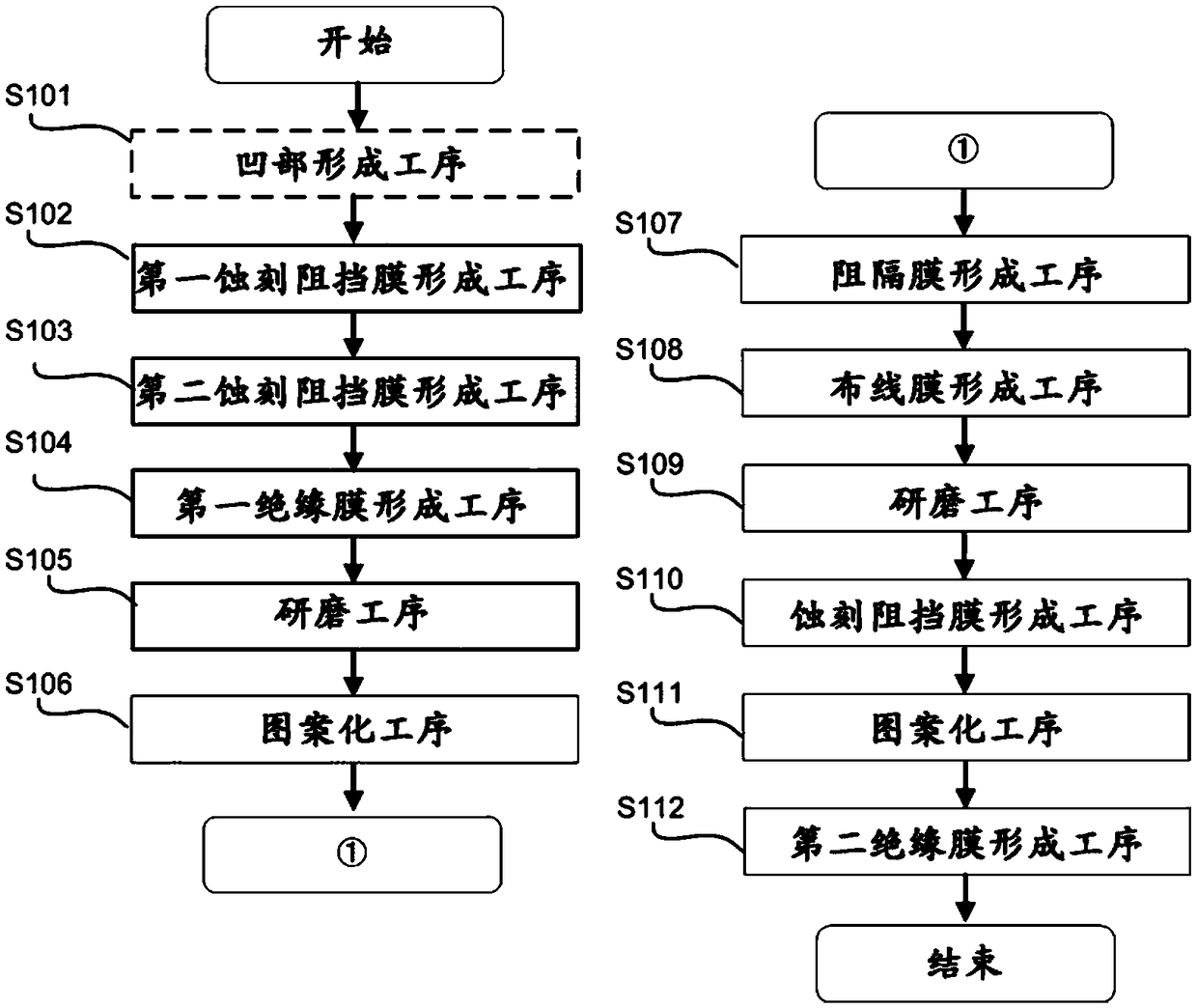
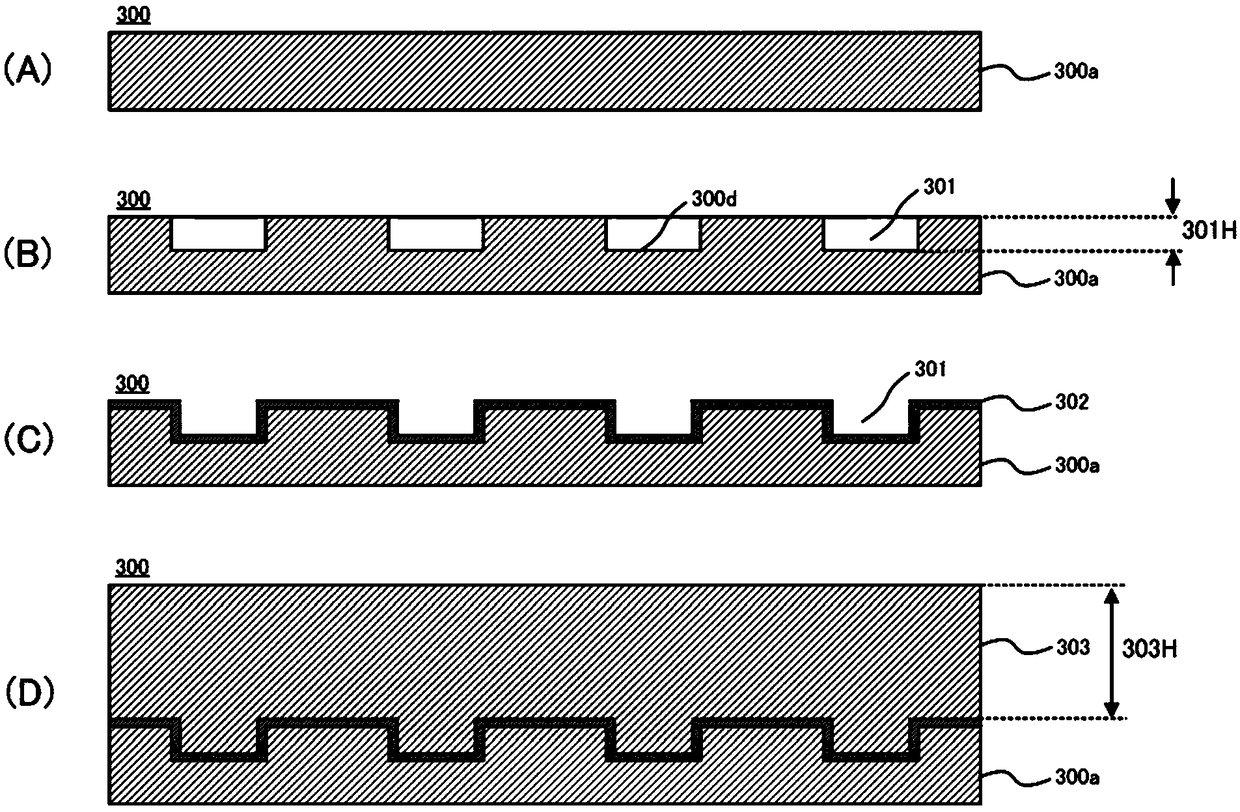
[0031] use Figure 1 ~ Figure 6 , Describe a step of the manufacturing process of a semiconductor device. figure 1 Is a flowchart of the manufacturing process of a semiconductor device, Figure 2 ~ Figure 6 To show and figure 1 The state of the substrate corresponding to each process.
[0032] (Depression forming step S101)
[0033] The recess forming step S101 will be described.
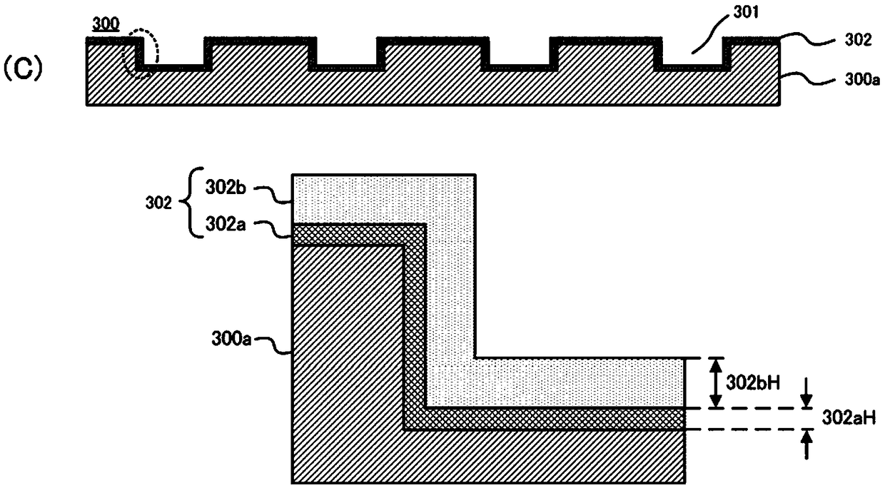
[0034] Regarding the recess forming step S101, use figure 2 (A) and (B) are explained. The first recess 301 is formed on the surface of the surface layer 300 a of the substrate 300. The surface layer 300a is composed of either or both of the insulating film and the Si substrate. The insulating film is, for example, a silicon oxide film (SiOC film) containing carbon. The first recess 301 is formed by a patterning technique. Here, the height (depth) 301H of the recess is formed to be larger than the total film thickness (302...
PUM
 Abstract
Description
Claims
Application Information
 - R&D
- Intellectual Property
- Life Sciences
- Materials
- Tech Scout
- Unparalleled Data Quality
- Higher Quality Content
- 60% Fewer Hallucinations
Browse by: Latest US Patents, China's latest patents, Technical Efficacy Thesaurus, Application Domain, Technology Topic, Popular Technical Reports.
© 2025 PatSnap. All rights reserved.Legal|Privacy policy|Modern Slavery Act Transparency Statement|Sitemap|About US| Contact US: help@patsnap.com