CMOS image sensor and production method thereof

A technology of image sensor and manufacturing method, which is applied in the direction of electric solid-state devices, semiconductor devices, radiation control devices, etc., can solve the problems of increasing costs and achieve cost-saving effects

Active Publication Date: 2018-11-13
SHANGHAI HUALI INTEGRATED CIRCUTE MFG CO LTD
View PDF3 Cites 5 Cited by
  • Summary
  • Abstract
  • Description
  • Claims
  • Application Information

AI Technical Summary

Problems solved by technology

Therefore, in the prior art, the introduction of the P-type doped isolation region 102 will increase the cost

Method used


Image

  • CMOS image sensor and production method thereof
  • CMOS image sensor and production method thereof
  • CMOS image sensor and production method thereof

Examples


Embodiment Construction

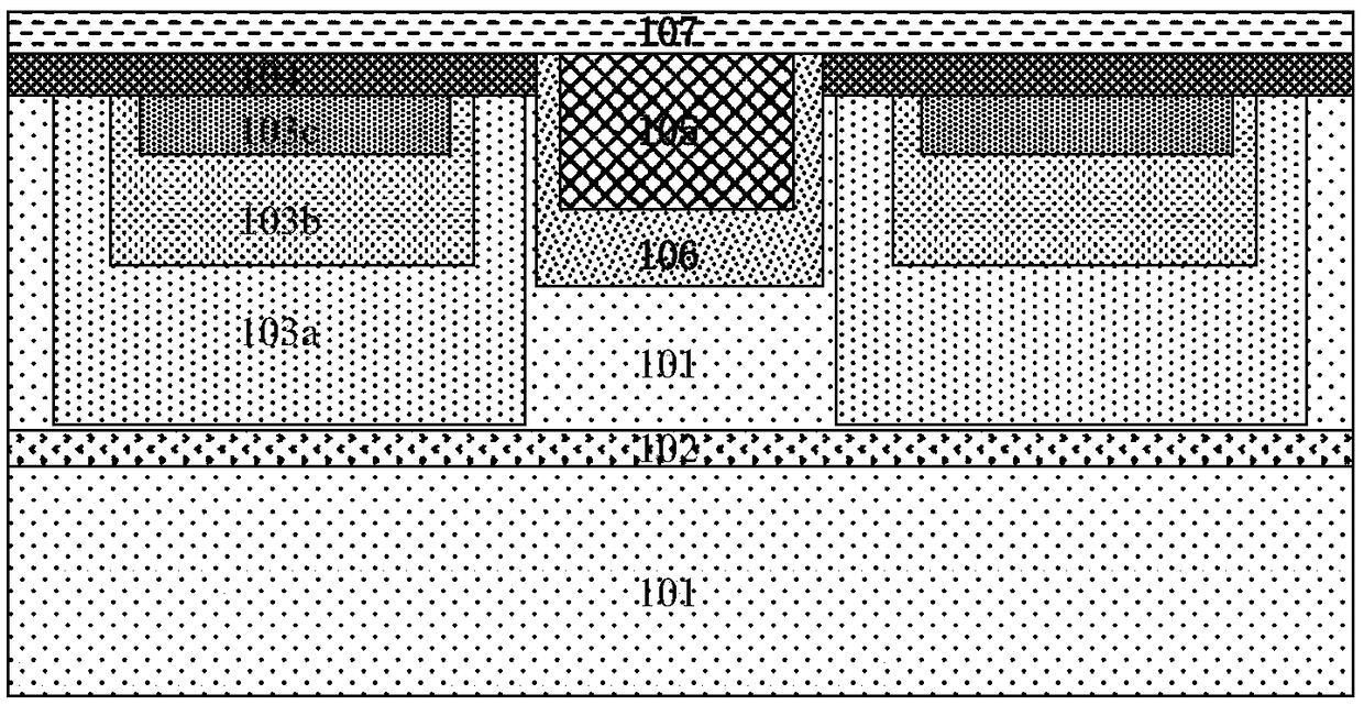
[0045] Such as Figure 4 Shown is a schematic structural diagram of photosensitive diodes of each pixel unit of the CMOS image sensor of the embodiment of the present invention. The CMOS image sensor of the embodiment of the present invention is formed on a P-type semiconductor substrate 1 and includes a plurality of pixel units.

[0046] Each of the pixel units includes a surface clamped photodiode, and the clamped photodiode includes an N-type buried layer formed in the P-type semiconductor substrate 1 and a surface P+ layer 4 formed on the surface of the N-type buried layer. And the clamping photodiode is formed by stacking the P-type semiconductor substrate 1 , the N-type buried layer and the surface P+ layer 4 .

[0047] In the embodiment of the present invention, the N-type buried layer includes a deep N well 3a, an N well 3b and a surface N-type layer 3c, the junction depth of the deep N well 3a is greater than the junction depth of the N well 3b and the N The well 3b ...


PUM


Abstract

The invention discloses a CMOS image sensor, which is formed on a P-type semiconductor substrate and comprises a plurality of pixel units, wherein each pixel unit comprises a surface clamp photodiode;each clamp photodiode comprises an N-type buried layer formed in the P-type semiconductor substrate and a surface P+ layer formed on the surface of the N-type buried layer; field oxide layers are formed on the surface of the P-type semiconductor substrate between the adjacent surface clamp photodiodes; a first P-type doped isolation region is formed at the bottom of each field oxide layer; a fully injected second P-type doped isolation region is formed at the bottoms of the N-type buried layers; and the depths of the bottom surfaces of the first P-type doped isolation regions are greater thanor equal to that of the top surface of the second P-type doped isolation region, so that the bottoms of the first P-type doped isolation regions are overlapped with the second P-type doped isolationregion. The invention further discloses a production method of the CMOS image sensor. According to the CMOS image sensor, reduction of the cost under the condition of achieving noise isolation of thesubstrate can be ensured.

Description

technical field [0001] The invention relates to the field of semiconductor integrated circuit manufacturing, in particular to a CMOS image sensor; the invention also relates to a manufacturing method of the CMOS image sensor. Background technique [0002] The existing CMOS image sensor (CMOS Image Sensor, CIS) is composed of a pixel (Pixel) unit circuit and a CMOS circuit. Compared with the CCD image sensor, the CMOS image sensor has better integration because it adopts the CMOS standard manufacturing process, and can It is integrated on the same chip with other digital-analog calculation and control circuits, which is more suitable for future development. [0003] According to the number of transistors contained in the pixel unit circuit of the existing CMOS image sensor, it is mainly divided into 3T structure and 4T structure. [0004] Such as figure 1 Shown is a schematic diagram of an equivalent circuit of a pixel unit circuit of an existing 3T CMOS image sensor; the p...

Claims


Application Information

Patent Timeline
Patent Type & Authority Applications(China)
IPC IPC(8): H01L27/146
CPCH01L27/1463H01L27/14689
Inventor 李岩张武志
Owner SHANGHAI HUALI INTEGRATED CIRCUTE MFG CO LTD
Why Eureka
Try Eureka