A display panel and binding method

A technology of display panel and binding area, applied in the directions of printed circuit, printed circuit manufacturing, electric solid device, etc., can solve the problems of affecting the process, adhesion, unfavorable peeling, etc., to improve corrosion resistance, improve pressing accuracy, avoid The effect of line corrosion

Active Publication Date: 2019-11-15
WUHAN CHINA STAR OPTOELECTRONICS SEMICON DISPLAY TECH CO LTD
View PDF6 Cites 0 Cited by
  • Summary
  • Abstract
  • Description
  • Claims
  • Application Information

AI Technical Summary

Problems solved by technology

However, the existing countermeasure is to apply a layer of waterproof glue on the corrosion-prone area to isolate the air and moisture and meet the anti-corrosion requirements, such as Figure 1B As shown, the exposed part of the WOA wiring 104 is covered by the front waterproof glue 106, and the exposed part of the COF wiring 105 is covered by the back waterproof glue 107. Since the OLED industry needs to peel off the glass substrate 108, there will be two problems. One is The back waterproof adhesive 107 adheres to the glass substrate 108, which is not conducive to peeling off; the second is that after the glass substrate 108 is peeled off, the height of the back waterproof adhesive 107 exceeds the OLED layer 109, which affects subsequent manufacturing processes. Currently, the industry cannot overcome this problem. Apply the waterproof glue 107 on the back, its quality will be risky in the long run

Method used


Image

  • A display panel and binding method
  • A display panel and binding method
  • A display panel and binding method

Examples


Embodiment Construction

[0032] The following will clearly and completely describe the technical solutions in the embodiments of the present invention with reference to the drawings in the embodiments of the present invention. Apparently, the described embodiments are only some of the embodiments of the present invention, but not all of them. Based on the embodiments of the present invention, all other embodiments obtained by those skilled in the art without creative efforts fall within the protection scope of the present invention.

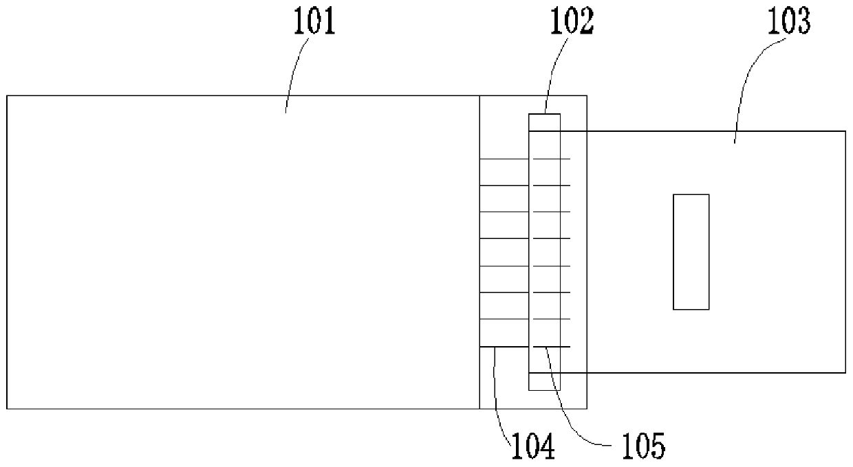
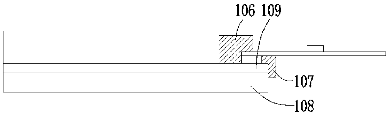
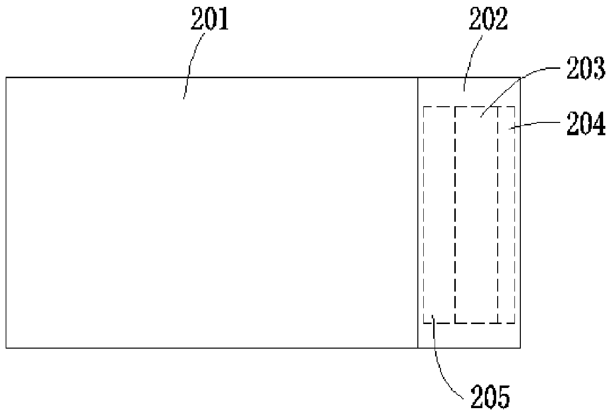
[0033] The present invention is aimed at the display panel of the prior art, because the back waterproof glue coated on the back bound to the signal wiring of the flexible circuit board and the display panel is adhered to the glass substrate, which is not conducive to peeling off, and the back waterproof glue after the glass substrate is peeled off The height exceeds the OLED layer and affects the technical problem of the subsequent manufacturing process. This embodiment...


PUM


Abstract

The present invention provides a display panel and a binding method. The display panel includes a display area and a non-display area located on one side of the display area. At least two signal wires are arranged in the non-display area. A binding area is set in the non-display area; the non-display area and the binding area have an overlapping area and a non-overlapping area, and the non-overlapping area located on one side of the binding area is the first area, which is relatively The non-overlapping area on the other side is the second area; the first area is provided with a waterproof adhesive layer, and the binding area is provided with a conductive adhesive layer; the conductive adhesive layer includes a conductive particle doped area, and a first insulating glue region located on one side of the conductive particle doped region, the first insulating glue region is located between the conductive particle doped region and the second region.

Description

technical field [0001] The invention relates to the technical field of display panel manufacturing, in particular to a display panel and a binding method. Background technique [0002] Mobile phones are used in a variety of environments, and some high-humidity and high-temperature environments are more corrosive to mobile phone screens, so the requirements for corrosion resistance of the screen are getting higher and higher. The module segment mainly lies in the flexible circuit (Chip On Film, COF) and The waterproof and anti-corrosion of the wires in the wire on array (WOA) area of ​​the bonding area of ​​the display panel. The traditional anti-corrosion method for WOA lines in the LCD manufacturing process is to apply waterproof glue on the front of the WOA lines and the back where the COF and WOA are bound for anti-corrosion. [0003] Such as Figure 1A-1B As shown, after the WOA wiring 104 arranged in the non-display area of ​​the display panel 101 and connected to the ...

Claims


Application Information

Patent Timeline
Patent Type & Authority Patents(China)
IPC IPC(8): H01L51/52H01L51/56
CPCH10K59/873H10K71/40H05K3/323H05K1/189H05K2201/10128H10K59/131H01L24/29H01L24/32H01L24/83H01L2224/29078H01L2224/29499H01L2224/32225H01L2224/83191H01L2224/83203H10K50/844
Inventor 吴建军
Owner WUHAN CHINA STAR OPTOELECTRONICS SEMICON DISPLAY TECH CO LTD
Why Eureka
Try Eureka