Sub-pixel-level PCB board defect reference point detection method

A PCB board and sub-pixel level technology, which is applied in the field of SMT high-speed and high-precision automatic placement machines, can solve the problem that the accuracy does not reach the sub-pixel level, and achieve the effects of enhancing accuracy, improving accuracy, and reducing mis-segmentation

Inactive Publication Date: 2018-11-16
JIANGSU UNIV
View PDF2 Cites 20 Cited by
  • Summary
  • Abstract
  • Description
  • Claims
  • Application Information

AI Technical Summary

Problems solved by technology

These methods have their unique applicability, but their precision has not reached the sub-pixel level, and with the development of science and technology, the requirements for precision are getting higher and higher

Method used


Image

  • Sub-pixel-level PCB board defect reference point detection method
  • Sub-pixel-level PCB board defect reference point detection method
  • Sub-pixel-level PCB board defect reference point detection method

Examples


Embodiment Construction

[0069] The present invention will be further described below in conjunction with the accompanying drawings and specific embodiments, but the protection scope of the present invention is not limited thereto.

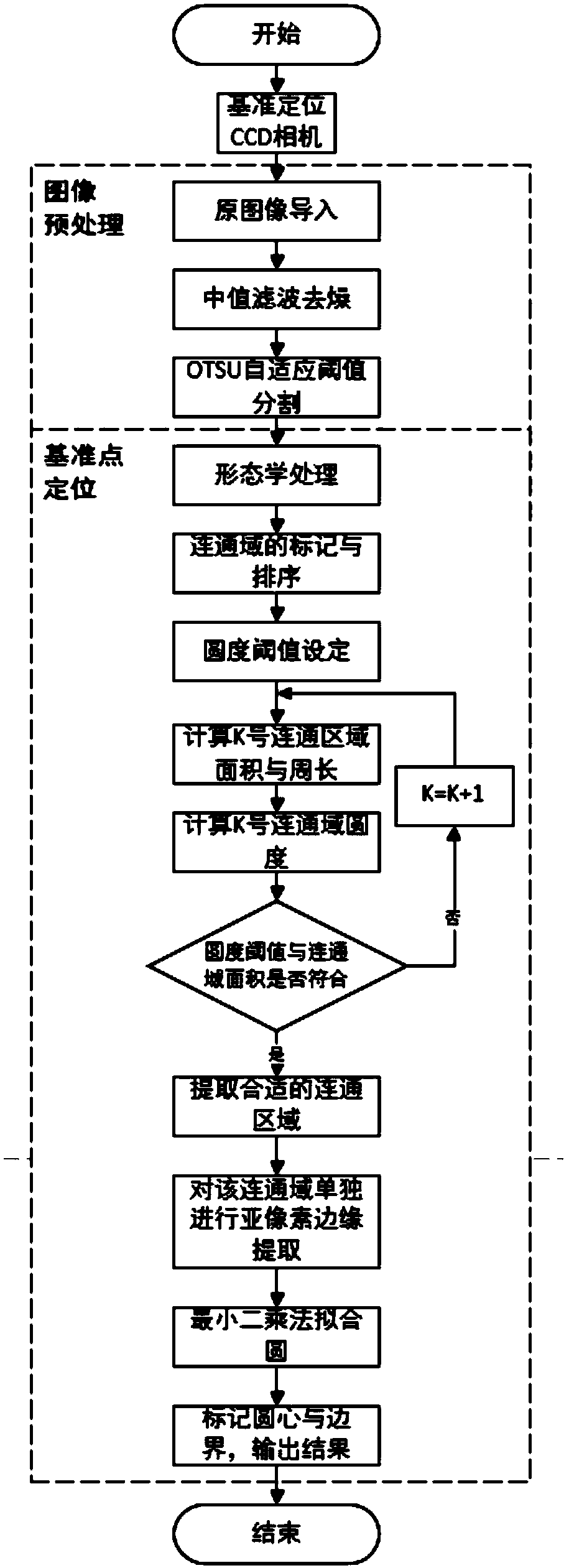
[0070] Such as figure 1 As shown, a sub-pixel level PCB board defect reference point detection method according to the present invention specifically includes the following steps:

[0071] S1. Acquisition of the original image: read in an original image 1 of the PCB board with a size of 480×640 through the reference positioning CCD camera, such as figure 2 shown;

[0072] S2, preprocessing the original image of the PCB board, including the following steps:

[0073] S2.1. Adaptive median filter denoising: perform median filter denoising on the target image to obtain denoised image 2; image 3 As shown, the specific steps are:

[0074] order z min = S xy The minimum gray value in z max = S xy The maximum gray value in z med = S xy The median gray value in z xy =...


PUM


Abstract

The invention provides a sub-pixel-level PCB board defect reference point detection method. The method comprises the following steps: reading in a PCB grayscale image 1; preprocessing the PCB image, wherein self-adaptive median filtering denoising is used to remove pepper-and-salt-type noises to obtain a denoised image 2, a method of maximum inter-class variance is used to carry out binary segmentation of the image to obtain a binarized image 3, and a mathematical morphology method is used to process the image to further remove small interference points and holes to obtain an image 4; using acommunicate-domain algorithm to obtain a position and a scale of a preprocessed image feature region; and then enabling reference circle extraction and positioning efficiency and precision to be improved through a sub-pixel edge detection algorithm and fitting of a least square method. Requirements of high-precision reference point extraction and positioning are effectively satisfied, defects of low precision and low speed of previous reference point positioning are overcome, and the method has the characteristics of high applicability and high accuracy.

Description

technical field [0001] The invention relates to the field of SMT high-speed and high-precision automatic placement machines, in particular to a sub-pixel-level PCB board defect reference point detection method. Background technique [0002] Surface mount technology SMT (Surface Mount Technology) is a new generation of electronic assembly technology, which compresses traditional electronic components into devices with only a few tenths of the volume. SMT surface mount technology mainly involves placement technology, welding technology, semiconductor packaging technology, assembly equipment design technology, circuit forming technology, functional design simulation technology, etc. The SMT production line mainly includes: placement machine, printing machine, SPI (solder paste inspection instrument), wave soldering equipment, reflow soldering equipment, AOI testing equipment (automatic optical inspection equipment), X-Ray testing equipment, rework workstation, etc. Among them,...

Claims


Application Information

Patent Timeline
Patent Type & Authority Applications(China)
IPC IPC(8): G06T7/00G06T7/13G06T7/136G06T7/70G01N21/88
CPCG01N21/8851G01N2021/8864G06T7/0006G06T2207/10004G06T2207/20032G06T2207/30141G06T7/13G06T7/136G06T7/70
Inventor 许桢英李世奇徐梦莹赵波王一凡
Owner JIANGSU UNIV
Why Eureka
Try Eureka