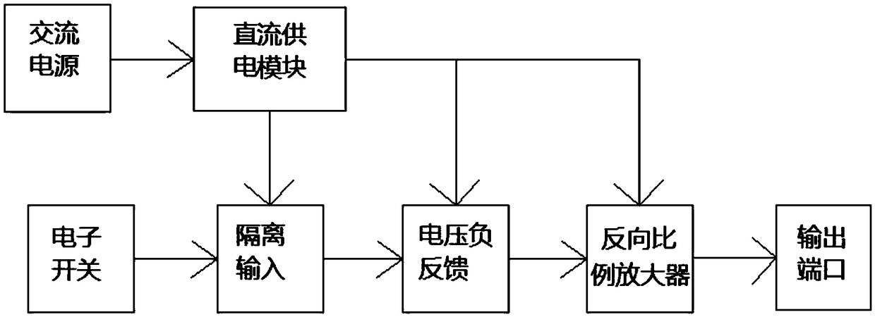
Switch quantity acquisition circuit
A switch value acquisition and circuit technology, applied in the field of switch value acquisition circuit, can solve the problems of poor signal acquisition effect, low accuracy, acquisition failure, etc., and achieve the effect of good reading, secondary control and good stability
- Summary
- Abstract
- Description
- Claims
- Application Information
AI Technical Summary
Problems solved by technology
Method used
Image
Examples
Embodiment 2
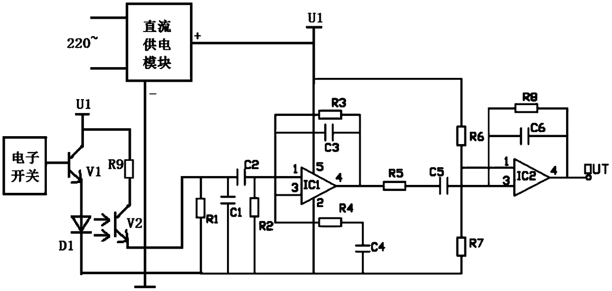
[0019] Embodiment 2, on the basis of embodiment 1, designed specific circuit diagram, as figure 2 As shown in the figure, the isolated input module includes a triode V1, a diode D1 and a triode V2. The signal of the electronic switch triggers the triode V1 to conduct. The signal is input to the voltage negative feedback module. The existence of resistors R1 and R2 can prevent self-excitation, and they are also input resistors. Capacitor C1 can prevent high-frequency interference from mixed signals, and short-circuit it when encountering high-frequency interference. Capacitor C2 is a signal coupling capacitor. The previous chip IC1 constitutes a voltage negative feedback circuit, R3 and R4 are feedback resistors, and the feedback voltage is sent to the inverting terminal of the chip IC1. C3 plays the role of frequency compensation: when the frequency is high, the capacitive reactance of C3 decreases, the total impedance of C3 and R3 decreases, and the feedback amount decrease...
PUM
 Abstract
Description
Claims
Application Information


