High electron mobility transistor with coupling field plates

A high electron mobility, transistor technology, applied in circuits, electrical components, semiconductor devices, etc., can solve the problems of uneven lateral electric field distribution, large lateral electric field front value of the source field plate, and low lateral voltage withstand capability of the device. Achieve the effects of optimized electric field distribution, low lateral withstand voltage capability, and fast switching speed

Active Publication Date: 2018-11-20
济南半一电子有限公司
View PDF9 Cites 0 Cited by
  • Summary
  • Abstract
  • Description
  • Claims
  • Application Information

AI Technical Summary

Problems solved by technology

High electron mobility transistor structures using conventional source field plate technology such as figure 1 As shown, since the traditional source field plate is formed by the source electrode, its potential is a fixed source potential, resulting in a large lateral electric field peak at the end of the source field plate, and in the barrier layer between the gate electrode and the drain electrode The distribution of the lateral electric field is very uneven, so that the lateral withstand voltage capability of the device is low, and the breakdown voltage of the device is much lower than the theoretical value

Method used


Image

  • High electron mobility transistor with coupling field plates
  • High electron mobility transistor with coupling field plates

Examples


Embodiment Construction

[0022] The present invention will be further introduced below in conjunction with the accompanying drawings and specific embodiments.

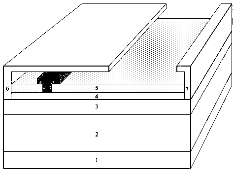
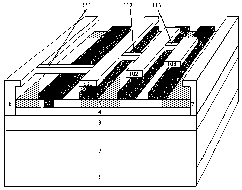
[0023] The invention discloses a high electron mobility transistor with a coupling field plate, comprising: a substrate 1; a buffer layer 2 is arranged above the substrate 1; a channel layer 3 is arranged above the buffer layer 2; and a channel layer 3 is arranged above the channel layer 3 A source electrode 6, a drain electrode 7 and a barrier layer 4 are provided, and the source electrode 6 and the drain electrode 7 are located at both ends of the barrier layer 4, and the barrier layer 4 is located in the middle of the source electrode 6 and the drain electrode 7; the barrier layer 4, a dielectric layer 5 and a gate electrode 8 are arranged above; it is characterized in that several coupling field plates are arranged on the surface of the dielectric layer 5 between the gate electrode 8 and the drain electrode 7, and all coupling field plates ...


PUM


Abstract

The present invention provides a high electron mobility transistor with coupling field plates. The transistor comprises a substrate. A buffer layer is arranged on the substrate, a channel layer is arranged on the buffer layer, a source electrode, a drain electrode and a barrier layer is arranged on the channel layer, the source electrode and the drain electrode are located on both ends of the barrier layer, and the barrier layer is located between the source electrode and the drain electrode. A dielectric layer and a gate electrode are arranged on the barrier layer. The surface of dielectric layer, between the gate electrode and the drain electrode, is provided with a plurality of coupling field plates, a coupling electrode is arranged on each coupling field plate, and each coupling electrode is connected with the source electrode via the corresponding metal interconnecting wire. According to the transistor, the coupling potential of each coupling field plates is changed via the size design of the corresponding coupling electrode and the corresponding coupling field plate, so that the regulating effect of coupling field plates on transverse electric field(s) is changed, the transverse electric field distribution of device(s) is optimized, and the transverse voltage endurance capability of the device(s) is improved.

Description

technical field [0001] The present invention relates to the field of power semiconductor devices, and more specifically relates to a high electron mobility transistor with coupled field plates suitable for high voltage applications. Background technique [0002] High Electron Mobility Transistors (HEMTs) with heterostructures, especially those made of GaN and AlGaN, feature high electron mobility and a large critical electric field, resulting in a high breakdown voltage , The advantages of small on-resistance and fast switching speed can improve the efficiency of the power management system and reduce the volume of the power management system, and have broad application prospects in the field of power semiconductors. [0003] Due to the technical difficulty and high cost of forming P-type doped regions in heterostructure high electron mobility transistors, super junction technology and buried layer technology in the field of power semiconductors cannot be applied to HEMT dev...

Claims


Application Information

Patent Timeline
Patent Type & Authority Applications(China)
IPC IPC(8): H01L29/778H01L21/335H01L29/40
CPCH01L29/402H01L29/66462H01L29/778
Inventor 张春伟李阳岳文静李志明付小倩
Owner 济南半一电子有限公司
Why Eureka
Try Eureka