Method of cutting silicon wafer

A technology for silicon wafers and cutting machines, which is applied to fine working devices, grinding machines, metal processing equipment, etc., and can solve problems such as low cutting efficiency

Inactive Publication Date: 2018-11-23
阜宁协鑫光伏科技有限公司
View PDF6 Cites 6 Cited by
  • Summary
  • Abstract
  • Description
  • Claims
  • Application Information

AI Technical Summary

Problems solved by technology

[0004] Based on this, it is necessary to provide a new method for cutting silicon wafers to solve the problem of low cutting efficiency of traditional diamond wire sawing silicon wafers

Method used


Image

  • Method of cutting silicon wafer
  • Method of cutting silicon wafer
  • Method of cutting silicon wafer

Examples


Embodiment 1

[0040] A method for cutting a silicon wafer, comprising the steps of:

[0041]A silicon block with a thickness of 156 mm and a cross-sectional size of 156×156 mm is selected, and the cross-sectional diameter of the diamond wire is selected to be 70 μm.

[0042] Install the crystal holder with the silicon block attached on the workbench of the silicon block cutting machine above the diamond wire mesh;

[0043] The guide wheel drives the diamond wire attached to it to move until the linear speed of the diamond wire reaches a predetermined value;

[0044] Press down the workbench, and at the same time, the guide wheel of the silicon block cutting machine drives the diamond wire to reciprocate, and the diamond wire grinds and cuts the silicon block. See Table 1 for other parameters.

[0045] Table 1

[0046] parameter

[0047] The cutting time for each cut is 130 minutes.

Embodiment 2

[0049] A silicon block and a diamond wire of the same size as in Example 1 are selected for use. The method for cutting silicon wafers is substantially the same as in Example 1, except that the cutting parameters are different, as shown in Table 2:

[0050] Table 2

[0051] parameter

[0052] The cutting time for each cut is 122 minutes.

Embodiment 3

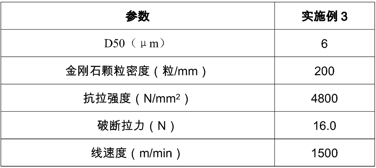
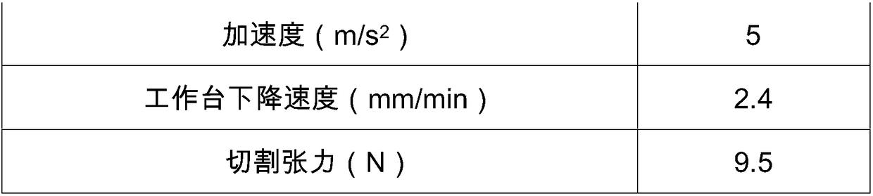
[0054] A silicon block and a diamond wire of the same size as in Example 1 are selected for use. The method for cutting silicon wafers is substantially the same as in Example 1, except that the cutting parameters are different, as shown in Table 3:

[0055] table 3

[0056]

[0057]

[0058] The cutting time per cut is 113 minutes.


PUM

PropertyMeasurementUnit
Particle sizeaaaaaaaaaa
Tensile strengthaaaaaaaaaa
Section diameteraaaaaaaaaa

Abstract

The invention relates to a method of cutting a silicon wafer. The method comprises the following steps: mounting a crystal tray where the silicon wafer is attached on a worktable of a silicon briquette cutter above a diamond wire screen; driving a diamond wire attached to the diamond wire screen by a guide wheel till the linear velocity of the diamond wire reaches a preset value; and pressing theworktable and driving the diamond wire by the guide wheel of the silicon briquette cutter to perform a reciprocating motion, wherein the diamond wire grinds and cuts the silicon briquette; the particle diameter D50 of diamond powder forming the diamond wire is 5.5-8.5 [mu]m, the particle density of the diamond powder of the diamond wire is 150-250 / mm, in the cutting process, the preset value of the linear velocity of the diamond wire is 1200-2000 m / min, and the pressing velocity of the worktable is 0.5-3.5 mm / min.

Description

technical field [0001] The invention relates to the field of cutting silicon wafers, in particular to a method for cutting silicon wafers. Background technique [0002] In recent years, the technological development of the solar photovoltaic industry is changing with each passing day, especially the silicon wafer cutting link, which is the main production link of the solar photovoltaic industry. In the silicon wafer cutting process, technological innovations such as mortar free abrasive linear cutting, mortar free abrasive structural wire cutting, and diamond wire bonded abrasive cutting have been successively experienced. Since the cutting efficiency far exceeds that of mortar cutting, and the loss of silicon material is significantly reduced, diamond wire bonded abrasives have become the most important cutting method for solar photovoltaic slices. [0003] However, the cutting efficiency of traditional diamond wire cut silicon wafers is low, which is far from meeting the ...

Claims


Application Information

Patent Timeline
IPC IPC(8): B28D5/04B24B27/06
CPCB24B27/0633B24B27/0675B28D5/045
Inventor 丁海军
Owner 阜宁协鑫光伏科技有限公司
Why Eureka
Try Eureka