Check patentability & draft patents in minutes with Patsnap Eureka AI!

SOI-based signal chip transverse integrated HBT and CMOS epitaxial structure and preparation method thereof

An epitaxial structure and lateral technology, applied in semiconductor/solid-state device manufacturing, electrical components, electrical solid-state devices, etc., can solve problems such as increased power consumption, high price, increased packaging structure and circuit complexity, etc., to increase flexibility , the effect of improving performance

Active Publication Date: 2018-11-23
BEIJING UNIV OF TECH
View PDF4 Cites 1 Cited by
  • Summary
  • Abstract
  • Description
  • Claims
  • Application Information

AI Technical Summary

Problems solved by technology

[0006] The PD module of the mobile phone integrates HBT devices and CMOS devices with independent chips, which not only increases the complexity of the packaging structure and circuit, but also increases power consumption. People hope that high-speed HBT devices and analog devices can be integrated into a single chip.
[0007] At present, HBT devices are mainly prepared with GaAs-based substrates, while CMOS devices are grown on Si-based substrates. Due to the small size of GaAs-based substrates, the preparation is complicated and expensive.

Method used


Image

  • SOI-based signal chip transverse integrated HBT and CMOS epitaxial structure and preparation method thereof
  • SOI-based signal chip transverse integrated HBT and CMOS epitaxial structure and preparation method thereof
  • SOI-based signal chip transverse integrated HBT and CMOS epitaxial structure and preparation method thereof

Examples


Embodiment Construction

[0035]In order to make the purpose, technical solutions and advantages of the embodiments of the present invention clearer, the technical solutions in the embodiments of the present invention will be clearly and completely described below in conjunction with the drawings in the embodiments of the present invention. Obviously, the described embodiments It is a part of embodiments of the present invention, but not all embodiments. Based on the embodiments of the present invention, all other embodiments obtained by persons of ordinary skill in the art without making creative efforts belong to the protection scope of the present invention.

[0036] Below in conjunction with accompanying drawing, the present invention is described in further detail:

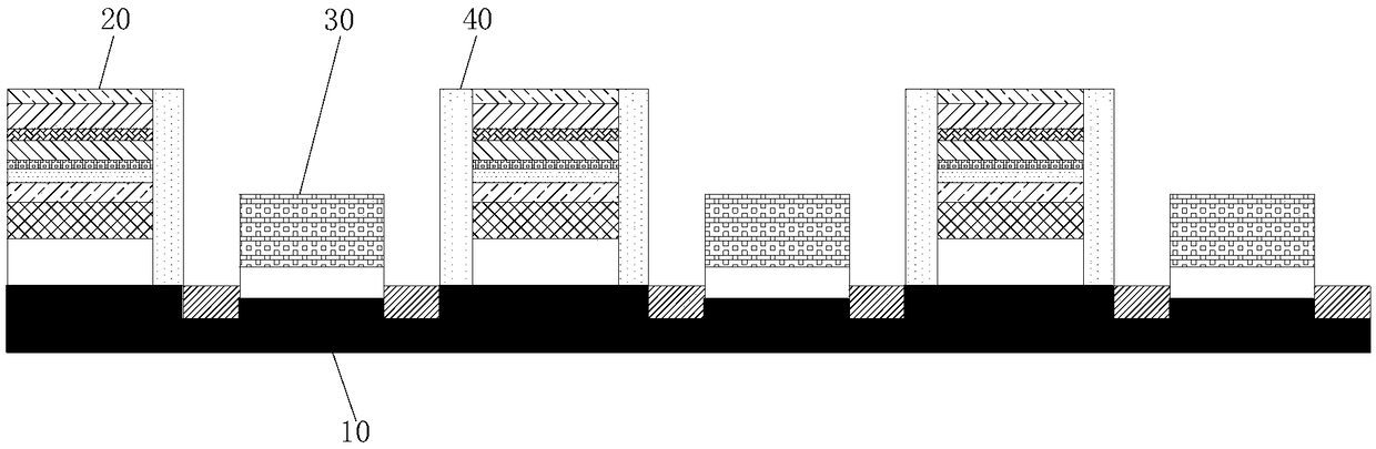
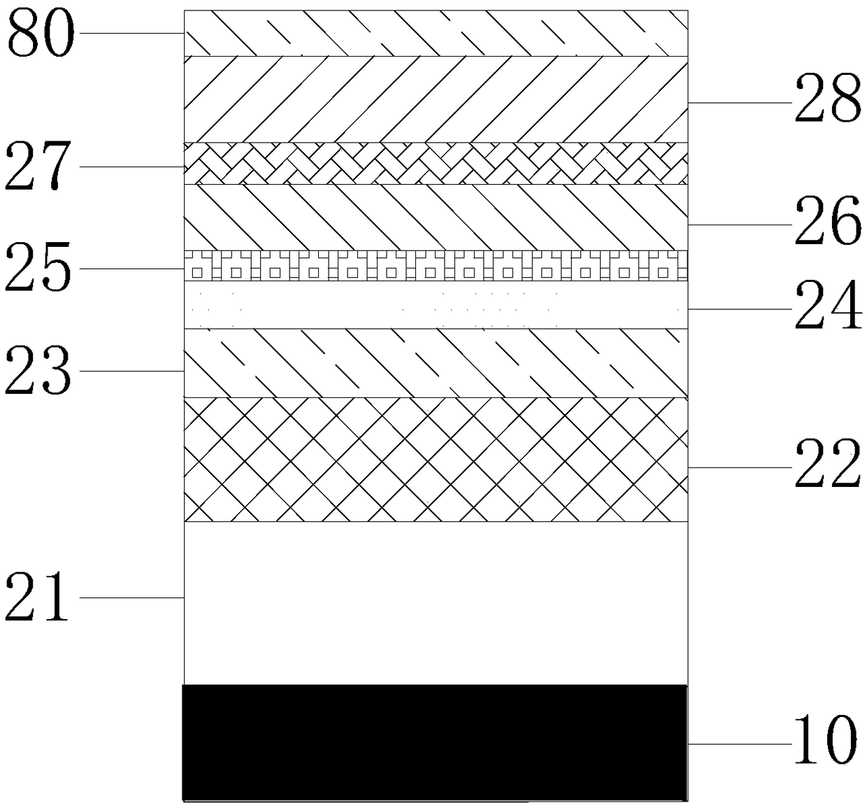
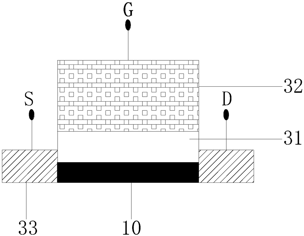
[0037] Such as Figure 1-3 As shown, the present invention provides an epitaxial structure of SOI-based monolithic lateral integration of HBT and CMOS. The epitaxial structure is composed of multiple GaAs-based HBTs 20 and multiple C...


PUM


Abstract

The invention discloses an SOI-based signal chip transverse integrated HBT and CMOS epitaxial structure and a preparation method thereof. The epitaxial structure is constituted by a plurality of GaAs-based HBTs and a plurality of CMOSs which are all transversely integrated on the same SOI substrate. The preparation method comprises the steps that an InGaAs buffering layer is grown on an SOI substrate base, then all layers are sequentially grown on the InGaAs buffering layer to obtain the HBTs, InGaP corrosion isolation layers are grown on the HBTs, and then patterning is conducted; an HBT epitaxial structure area and an SOI surface Si layer are formed on the SOI substrate, and a CMOS structure is grown on an exposed SOI surface Si layer area; and through corresponding epitaxial and material deposition technologies, the purpose of single chip transverse integrating of SOI-based HBT and CMOS devices can be achieved. The SOI-based signal chip transverse integrated HBT and CMOS epitaxial structure and the preparation method thereof can be applied into 5G communication so as to realize single chip integration of power amplifier devices and analog devices.

Description

technical field [0001] The invention relates to the technical field of semiconductor device integration, in particular to the epitaxial structure and preparation method of SOI-based monolithic lateral integration of HBT and CMOS. Background technique [0002] In recent decades, the semiconductor process has been improving its performance through the continuous reduction of geometric size. The continuous reduction of size not only puts forward higher and higher requirements for equipment and processing technology, but also increases the cost, and due to the limitation of the inherent characteristics of silicon materials , the device speed of silicon process technology has approached the physical limit, further increasing the device speed and maintaining device linearity have faced great scientific and technical problems, without good linear characteristics, high-performance analog integrated circuits have encountered a gap between speed, precision and performance fundamental ...

Claims


Application Information

Patent Timeline
Patent Type & Authority Applications(China)
IPC IPC(8): H01L27/12H01L21/84
CPCH01L21/84H01L27/1203
Inventor 代京京王智勇兰天李颖
Owner BEIJING UNIV OF TECH
Features
  • R&D
  • Intellectual Property
  • Life Sciences
  • Materials
  • Tech Scout
  • Unparalleled Data Quality
  • Higher Quality Content
  • 60% Fewer Hallucinations
Learn More