LED chip and manufacturing method thereof

A technology of LED chips and manufacturing methods, which is applied to electrical components, circuits, semiconductor devices, etc., can solve the problems of limiting the improvement of the external quantum efficiency of LED chips, limiting the brightness of chips, etc., to achieve the improvement of current expansion ability, reduce the probability of occurrence, reduce The effect of reflection and absorption

Active Publication Date: 2018-11-23
XIAMEN CHANGELIGHT CO LTD
View PDF6 Cites 6 Cited by
  • Summary
  • Abstract
  • Description
  • Claims
  • Application Information

AI Technical Summary

Problems solved by technology

Therefore, the structure in the prior art limits the further improvement of chip brightness
[0005] In addition, since the common transparent conductive layer ITO is deposited by sputtering or evaporat

Method used


Image

  • LED chip and manufacturing method thereof
  • LED chip and manufacturing method thereof
  • LED chip and manufacturing method thereof

Examples


Embodiment Construction

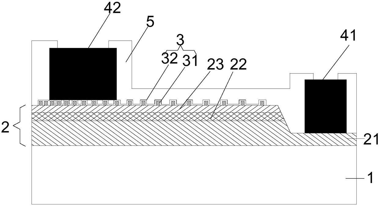
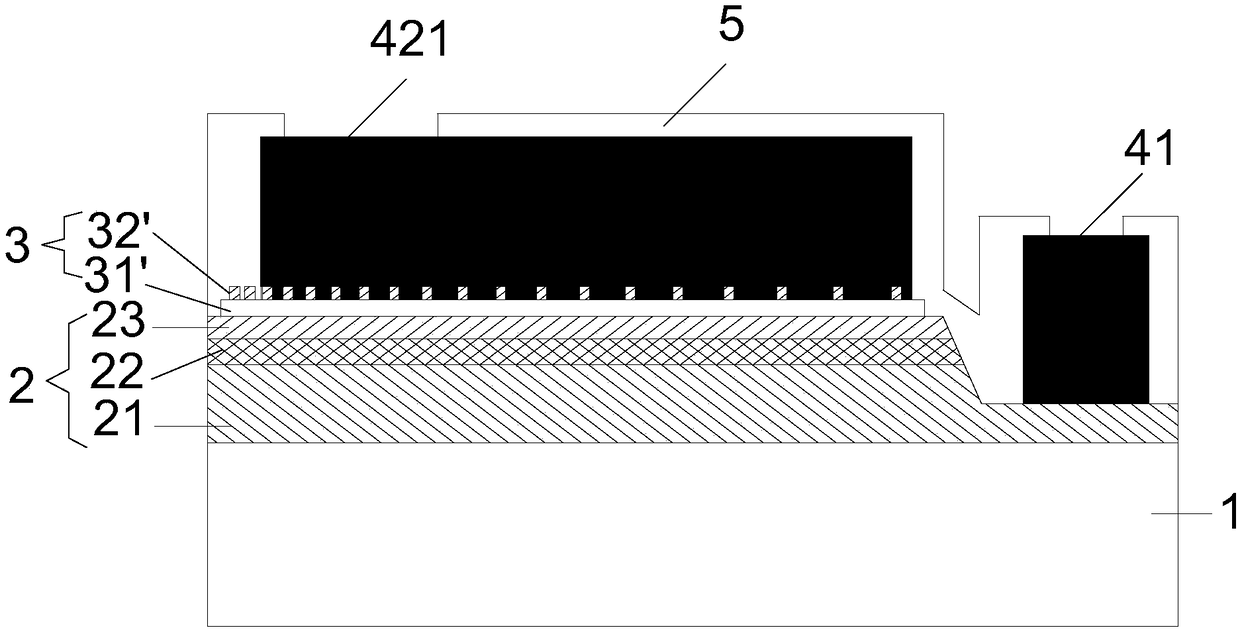
[0053] As mentioned in the background technology section, although the current spreading layer is added in the prior art, the current distribution of the LED chip can be made more uniform, thereby improving the luminous efficiency, but with the increase of the chip size, the semiconductor transparent conductive oxide current Scalability is limited. Although the further addition of metal interdigitated electrodes can further increase the uniformity of current spreading, it also introduces the problem of blocked light, which limits the further improvement of the brightness of the LED chip. At the same time, there is still a large amount of total reflection when the light exits from the entire transparent conductive oxide layer, which affects the off-chip quantum efficiency.

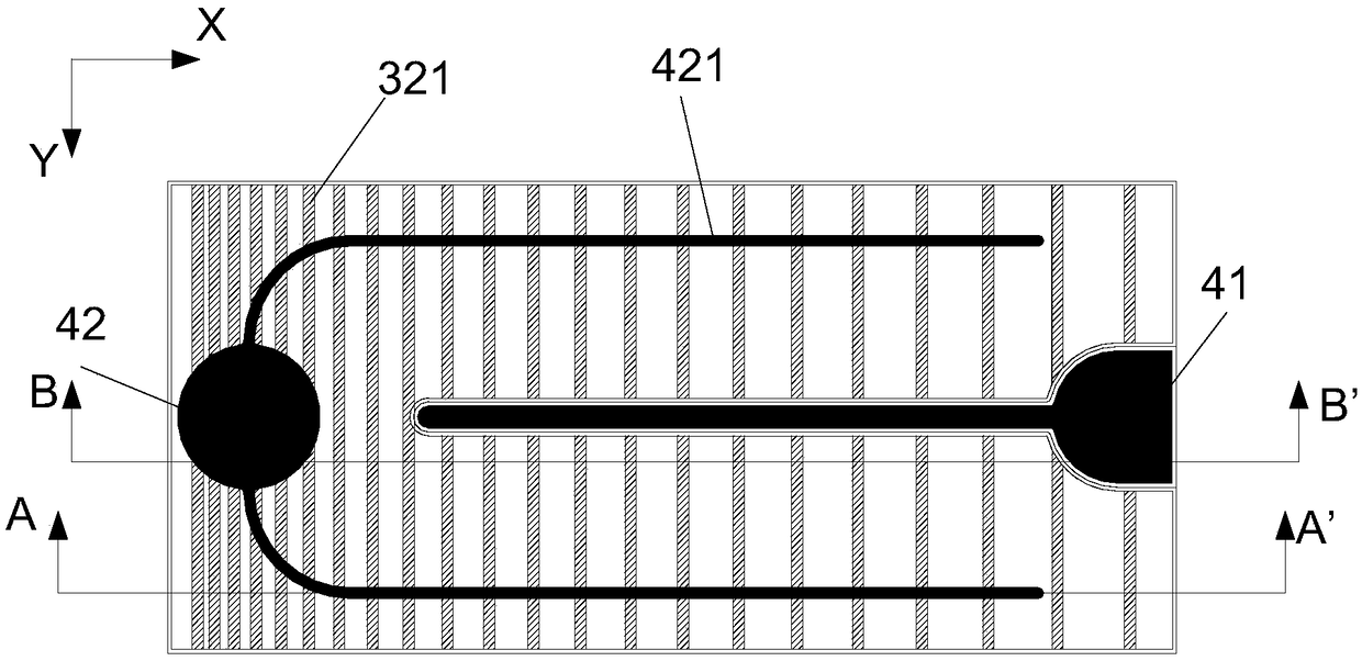
[0054] Based on this, the present invention provides a transparent interdigitated electrode design, which can not only further improve the current uniformity on the surface of the chip, but also form a step...


PUM

PropertyMeasurementUnit
Thicknessaaaaaaaaaa

Abstract

The present application provides an LED chip and manufacturing method thereof, wherein the LED chip comprises a substrate, an LED epitaxial structure, and a transparent conductive layer on a surface of the LED epitaxial structure. The transparent conductive layer comprises two-layer structure, which are a first transparent conductive layer and a second transparent conductive layer locating on thefirst transparent conductive layer and deviating from a second-type semiconductor layer, wherein, one of the first transparent conductive layer and the second transparent conductive layer is a whole layer structure, and the other one is a patterned structure. That is, a current spreading layer on the LED chip of the invention comprises an entire current spreading layer and a patterned current spreading layer. The patterned transparent conductive layer has no shielding effect on the LED chip due to the transparent structure, and a plurality of transparent interdigital electrodes are added to anexisting LED chip through the guiding of the patterned transparent conductive layer, so that the current spreading capability is greatly improved.

Description

technical field [0001] The invention relates to a manufacturing method of a semiconductor device, in particular to an LED chip and a manufacturing method thereof. Background technique [0002] Light Emitting Diode (LED) is called the fourth generation lighting source or green light source. It has the characteristics of energy saving, environmental protection, long life and small size. It is widely used in various indications, displays, decorations, backlights, and general lighting. and city night scenes. [0003] Since the PN electrodes of conventional front-mounted LED chips are located on the same side of the chip, the current needs to be conducted laterally, and the phenomenon of current crowding inevitably occurs between the PN electrodes. In order to solve this problem, the transparent conductive layer becomes an essential structure of the LED chip on the same side as the electrode. Commonly used ITO material, as a transparent conductive oxide, ITO can provide more th...

Claims


Application Information

Patent Timeline
IPC IPC(8): H01L33/38H01L33/42
CPCH01L33/38H01L33/387H01L33/42H01L2933/0016
Inventor 邬新根李俊贤刘英策魏振东周弘毅
Owner XIAMEN CHANGELIGHT CO LTD
Why Eureka
Try Eureka