Avalanche commutation diode special for 16000A/200-400V welding machine and preparation method thereof
A technology of rectifier diode and manufacturing method, applied in semiconductor/solid-state device manufacturing, circuits, electrical components, etc., can solve the problems of parallel current sharing, small capacity of rectifier diodes, etc., to reduce power consumption, ensure reliability, and improve instantaneous heat dissipation effect of ability
- Summary
- Abstract
- Description
- Claims
- Application Information
AI Technical Summary
Problems solved by technology
Method used
Image
Examples
Embodiment 1
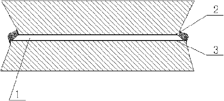
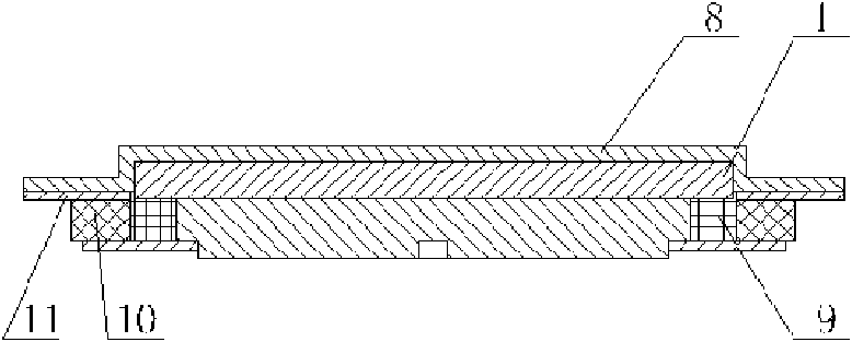
[0027] As shown in the figure, the special avalanche rectifier diode for electric welding machine is composed of a tube shell and a chip 1. The chip 1 includes a base area N and a phosphorous expansion area N. + and boron expansion area P + And cathode and anode titanium-nickel-gold (or titanium-nickel-silver) ohmic contacts 2 and 3, the thickness of the evaporated layer titanium: nickel: gold (or titanium: nickel: silver) is 0.2 μm: 0.5 μm: 0.1 μm, respectively, Tube thickness 5.5±0.5mm. Chip 1 adopts N-type (100) radial low-resistance single-crystal silicon wafer, resistivity ρn is 5-10Ω-cm, diameter is Φ70mm, thickness is 0.18±0.01mm, phosphorus expansion area N + and boron expansion area P + It is formed by two-sided primary diffusion.
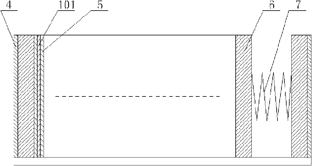
[0028] The manufacturing method of this special avalanche rectifier diode for electric welding machine is: adopt N-type (100) radial low-resistance monocrystalline silicon chip 101, described monocrystalline silicon chip 101 diameter is...
Embodiment 2
[0034] As shown in the figure, the special-purpose avalanche rectifier diode for electric welding machine is composed of a tube shell and a chip 1, and the chip 1 includes a base area N, a phosphorous expansion area N+ and a boron expansion area P+, and cathode and anode titanium-nickel-gold ( or titanium-nickel-silver) ohmic contacts 2 and 3, the thickness of titanium: nickel: gold (or titanium: nickel: silver) is respectively: 0.2μm: 0.5μm: 0.1μm, and the thickness of the tube is 5.5±0.5mm. Chip 1 adopts N-type (100) radial low-resistance single crystal silicon wafer, the resistivity ρn is 5-10Ω-cm, the diameter is 70mm, the thickness is 0.18±0.01mm, and the phosphorus expansion area N + and boron expansion area P + It is formed by two-sided primary diffusion.
[0035] The manufacturing method of this special avalanche rectifier diode for electric welding machine is: adopt N-type (100) radial low-resistance monocrystalline silicon chip 101, described monocrystalline silicon...
Embodiment 3
[0041] As shown in the figure, the special avalanche rectifier diode for electric welding machine is composed of a tube shell and a chip 1. The chip 1 includes a base area N and a phosphorous expansion area N. + and boron expansion area P + And cathode and anode titanium-nickel-gold (or titanium-nickel-silver) ohmic contacts 2 and 3, the thickness of titanium: nickel: gold (or titanium: nickel: silver) is 0.2μm: 0.5μm: 0.1μm, the thickness of the tube 5.5±0.5mmmm. Chip 1 is an N-type (100) radial low-resistance monocrystalline silicon wafer with a resistivity ρn of 5-10Ω-cm, a diameter of Φ70mm, and a thickness of 0.18±0.01mm. Phosphorus expansion zone N + and boron expansion area P + It is formed by two-sided primary diffusion.
[0042] The manufacturing method of this special avalanche rectifier diode for electric welding machine is: adopt N-type (100) radial low-resistance monocrystalline silicon chip 101, described monocrystalline silicon chip 101 diameter is 70mm, thi...
PUM
| Property | Measurement | Unit |
|---|---|---|
| Diameter | aaaaa | aaaaa |
| Thickness | aaaaa | aaaaa |
| Thickness | aaaaa | aaaaa |
Abstract
Description
Claims
Application Information


