Composite cover plate and preparation method thereof
A composite board and cover board technology, applied in electrical equipment shell/cabinet/drawer, electrical components, chassis/box/cabinet/drawer parts, etc., can solve the problems of single, poor thermal conductivity, easy deformation function, etc. Large space, enhanced thermal conductivity, reduced size effect
- Summary
- Abstract
- Description
- Claims
- Application Information
AI Technical Summary
Problems solved by technology
Method used
Image

Examples
preparation example Construction
[0044] This embodiment also relates to a method for preparing a composite cover plate, comprising the following steps:
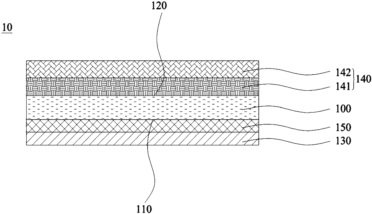
[0045] 1) Coating inorganic oxide, alkaline earth metal nitride, alkaline earth metal oxynitride, transition metal nitride, alkaline earth metal oxynitride, organic silicon or fluoride on the first surface of the substrate to form a hardened layer.
[0046] After the hardened layer is formed by coating, the hardness of the composite cover can be increased from 1H to 4H-5H.
[0047] In a specific example, the coating of inorganic oxides, alkaline earth metal nitrides, alkaline earth metal oxynitrides, transition metal nitrides, and alkaline earth metal oxynitrides on the first surface of the substrate is accomplished by vacuum coating. The silicone or fluoride is coated on the first surface of the substrate by means of spray coating or flow coating.
[0048] In a specific example, the hardened layer is a hard coating.
[0049] In a specific example, the mat...
Embodiment 1
[0064] The preparation method of the composite cover plate of the present embodiment is:
[0065] 1) Plating copper on the second surface of the substrate by electroplating, and then etching the copper plating layer by printing and etching ink to obtain a conductive layer;
[0066] 2) Print insulating material on the conductive layer to obtain a protective layer;
[0067] 3) performing surface treatment on the first surface of the substrate;
[0068] 4) spraying PMMA on the first surface of the substrate to obtain an adhesive layer;
[0069] 5) Spray silicone on the adhesive layer to form a 6 μm hardened layer;
[0070] 6) Carry out CNC processing and cleaning to obtain a composite cover plate (see attached figure 1 ).
Embodiment 2
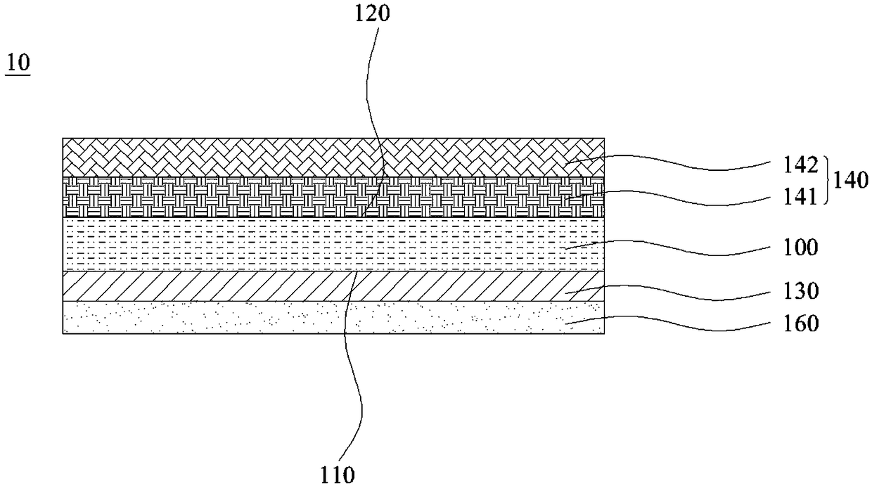
[0072] The preparation method of the composite cover plate of the present embodiment is:
[0073] 1) Plating copper on the second surface of the substrate by electroplating, and then etching the copper plating layer by printing and etching ink to obtain the first conductive layer;
[0074] 2) printing an insulating material on the first conductive layer to obtain a first protective layer;
[0075] 3) Continue copper plating on the first protective layer, and then etch the copper plating layer to generate an etching path to obtain a second conductive layer;
[0076] 4) printing an insulating material on the second conductive layer to obtain a second protective layer;
[0077] 5) performing surface treatment on the first surface of the substrate;
[0078] 6) Vacuum sputtering coating is carried out on the first surface of the substrate, and the coating material is SiO 2 、Si 3 N 4 、Si 2 N 2 A mixture of O to form a hardened layer of 0.8 μm;
[0079] 7) Spray an anti-finge...
PUM
| Property | Measurement | Unit |
|---|---|---|
| Nanohardness | aaaaa | aaaaa |
| Bending stress | aaaaa | aaaaa |
| Thermal conductivity | aaaaa | aaaaa |
Abstract
Description
Claims
Application Information
PatSnap Eureka turns technology decisions into work you can execute. Powered by our Innovation Knowledge Graph, it runs expert workflows across engineering, life sciences, materials and intellectual property. Get your review-ready output in minutes.


