
Liquid crystal display panel manufacturing method and liquid crystal display panel

A technology for liquid crystal display panels and manufacturing methods, applied in nonlinear optics, instruments, optics, etc., can solve problems such as uneven surface of color filter substrates, uneven diffusion of vertical alignment agents, and easy occurrence of bright spot defects, so as to improve liquid crystal alignment effect, avoid bad display, reduce the effect of bad display

Inactive Publication Date: 2018-11-27
SHENZHEN CHINA STAR OPTOELECTRONICS TECH CO LTD
View PDF7 Cites 12 Cited by
  • Summary
  • Abstract
  • Description
  • Claims
  • Application Information

AI Technical Summary

Problems solved by technology

However, there are still some defects when the vertical alignment agent is used for alignment. First, in order to expand the viewing angle, the existing liquid crystal display panels widely use pixel electrodes with a "rice" pattern, and slits are formed in the pixel electrodes. The position is not covered by the electrode material, and the passivation layer formed by silicon nitride or organic insulating material under the electrode layer is directly exposed. When the vertical alignment agent is used for alignment, the effect between the vertical alignment agent and the passivation layer The force is weaker than the force between the vertical alignment agent and the electrode, and it is easy to cause poor alignment, resulting in dark or bright line defects. Secondly, the color filter substrate of the existing liquid crystal display panel is generally formed with a color resist layer, a black matrix, and a common electrode. And spacers, after multiple film layers are stacked, a segment difference will be formed on the color filter substrate, resulting in uneven surface of the color filter substrate, with different terrains, and the vertical alignment agent cannot be uniformly diffused on the color filter substrate, which is prone to occurrence bright spot defect

Method used


Image

  • Liquid crystal display panel manufacturing method and liquid crystal display panel
  • Liquid crystal display panel manufacturing method and liquid crystal display panel
  • Liquid crystal display panel manufacturing method and liquid crystal display panel

Examples


Embodiment Construction

[0059] In order to further illustrate the technical means adopted by the present invention and its effects, the following describes in detail in conjunction with preferred embodiments of the present invention and accompanying drawings.

[0060] see Figure 9 , the invention provides a method for manufacturing a liquid crystal display panel, comprising the steps of:

[0061] Step S1, providing a first substrate 10 and a second substrate 20;

[0062] Specifically, the first substrate 10 is a TFT substrate. In the present invention, Color Filter on Array (COA) technology and Black Photo Spacer (BPS) technology are used to combine color resistance, black matrix and The spacers are all integrated on the first substrate 10 .

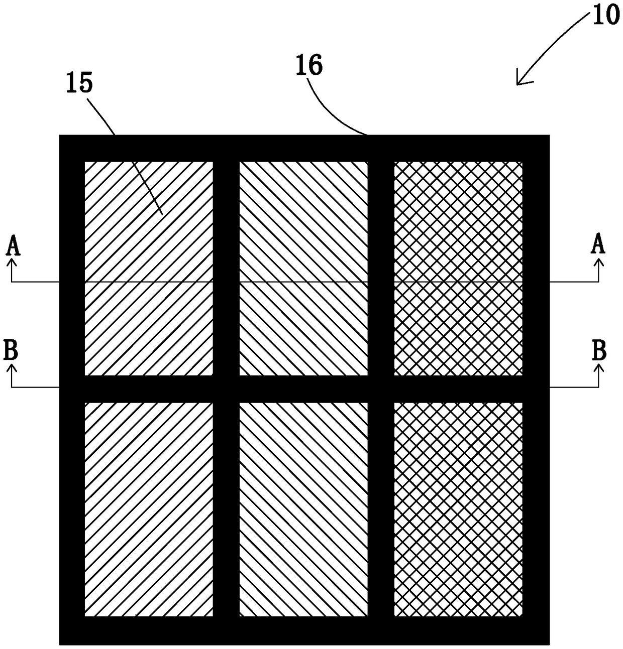
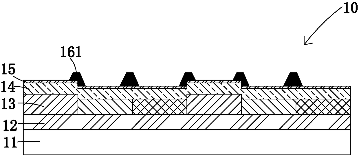
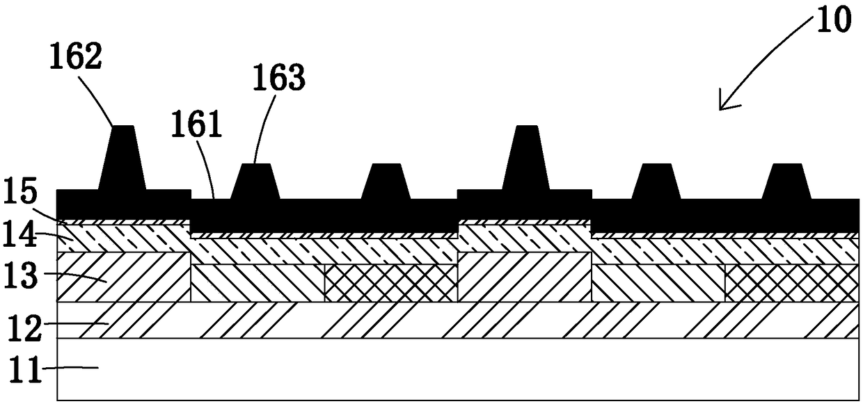
[0063] In detail, such as Figure 1 to Figure 3 As shown, the first substrate 10 includes a first base substrate 11, a TFT layer 12 disposed on the first base substrate 11, a color resist layer 13 disposed on the TFT layer 12, and a color resist layer 13 di...


PUM

PropertyMeasurementUnit
thicknessaaaaaaaaaa

Abstract

The invention provides a liquid crystal display panel manufacturing method and a liquid crystal display panel. The manufacturing method includes first providing a first substrate and a second substrate, wherein the first substrate is provided with a TFT layer, a color resistance layer, a pixel electrode layer and a light shielding layer, and only a common electrode is disposed on the second substrate; then forming an alignment film on the first substrate, coating a self-aligned liquid crystal material on the first substrate or the second substrate and pairing the first substrate and the secondsubstrate to form a liquid crystal box; then applying a voltage to the liquid crystal box while performing UV illuminating to enable the self-aligned liquid crystal material to undergo reverse polymerization to form a first polymer layer and a second polymer layer on the alignment film and the common electrode respectively. By means of the method, the self-aligned liquid crystal material can be diffused uniformly by improving the flatness of the substrates to avoid poor display.

Description

technical field [0001] The invention relates to the field of display technology, in particular to a method for manufacturing a liquid crystal display panel and the liquid crystal display panel. Background technique [0002] With the development of display technology, liquid crystal displays (Liquid Crystal Display, LCD) and other flat display devices are widely used in mobile phones, televisions, personal Various consumer electronic products such as digital assistants, digital cameras, notebook computers, and desktop computers have become the mainstream of display devices. [0003] Generally, a liquid crystal display panel includes a color filter (Color Filter, CF) substrate, a thin film transistor (Thin Film Transistor, TFT) substrate, and a liquid crystal (LC, Liquid Crystal) sandwiched between the color filter substrate and the thin film transistor substrate. On the CF substrate and the TFT substrate in the liquid crystal display panel, there is a layer of thin film mate...

Claims


Application Information

Patent Timeline
Patent Type & Authority Applications(China)
IPC IPC(8): G02F1/1337G02F1/1335
CPCG02F1/133512G02F1/133514G02F1/133703G02F1/133738
Inventor 兰松谢忠憬
Owner SHENZHEN CHINA STAR OPTOELECTRONICS TECH CO LTD
Learn More