

A power follower filter circuit
A technology of filter circuit and follower circuit, which is applied in the field of power supply follower filter circuit, can solve the problems of high cost of low-frequency ripple noise, inefficiency, cut off the effective DC component of power supply, etc., and achieve the effect of reducing power consumption
- Summary
- Abstract
- Description
- Claims
- Application Information
AI Technical Summary
Problems solved by technology
Method used
Image

Examples
Embodiment 1
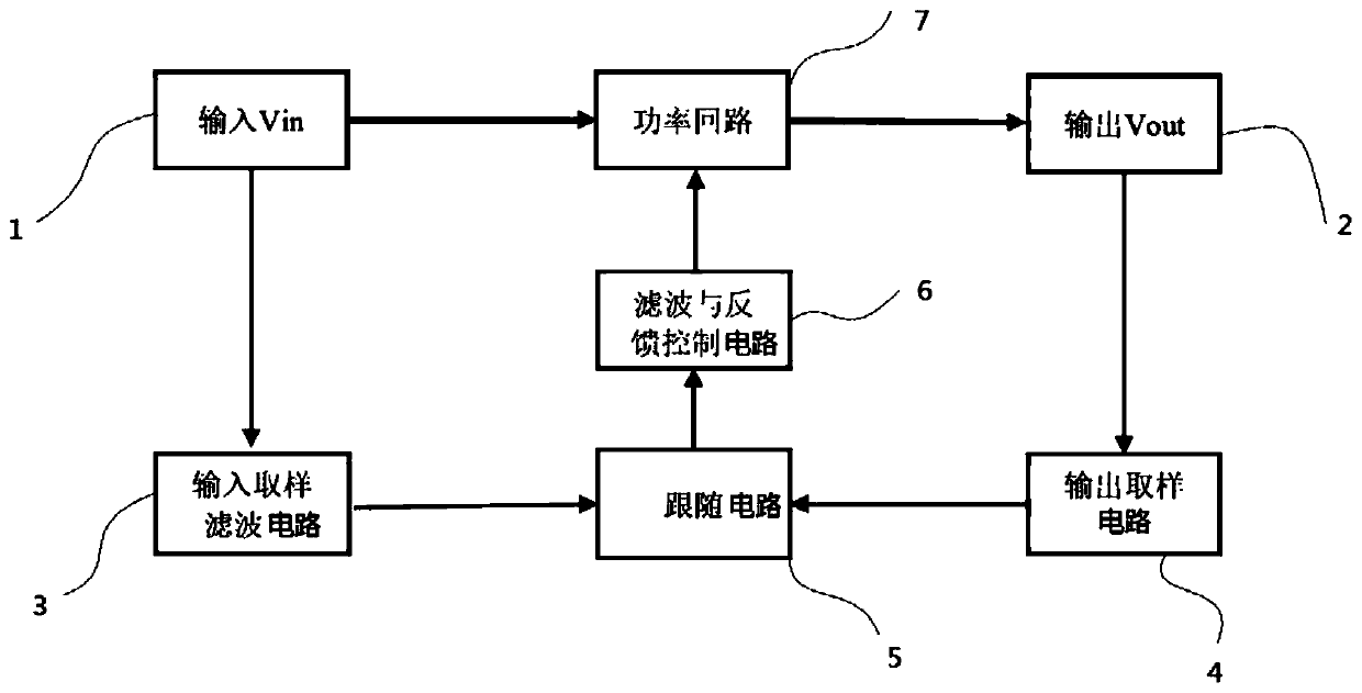
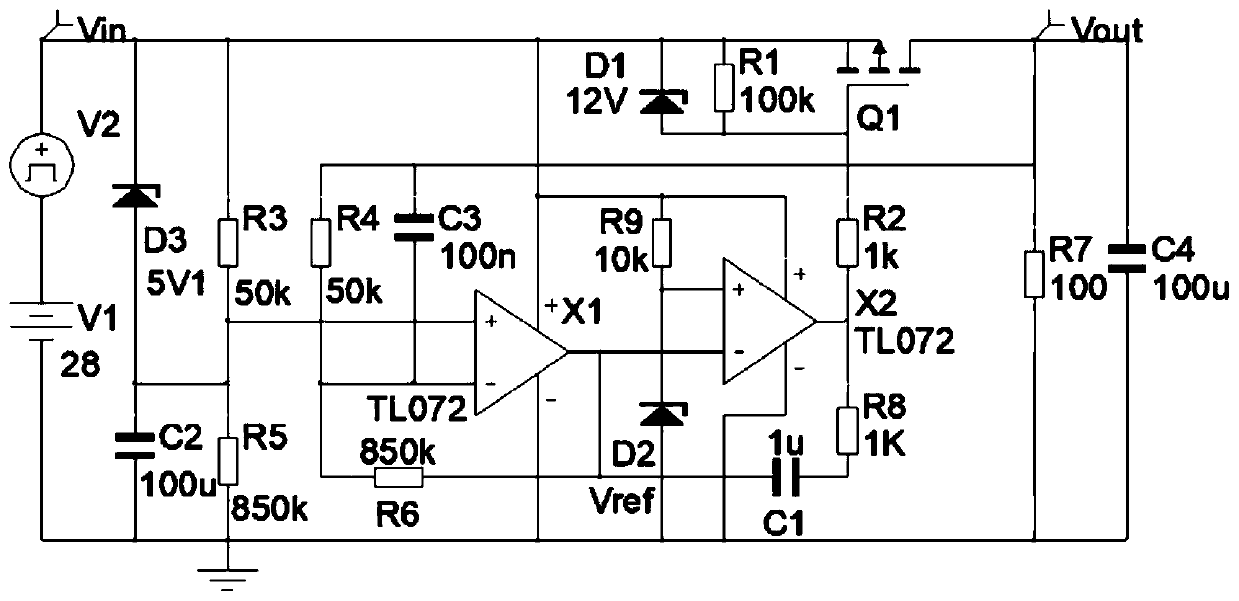
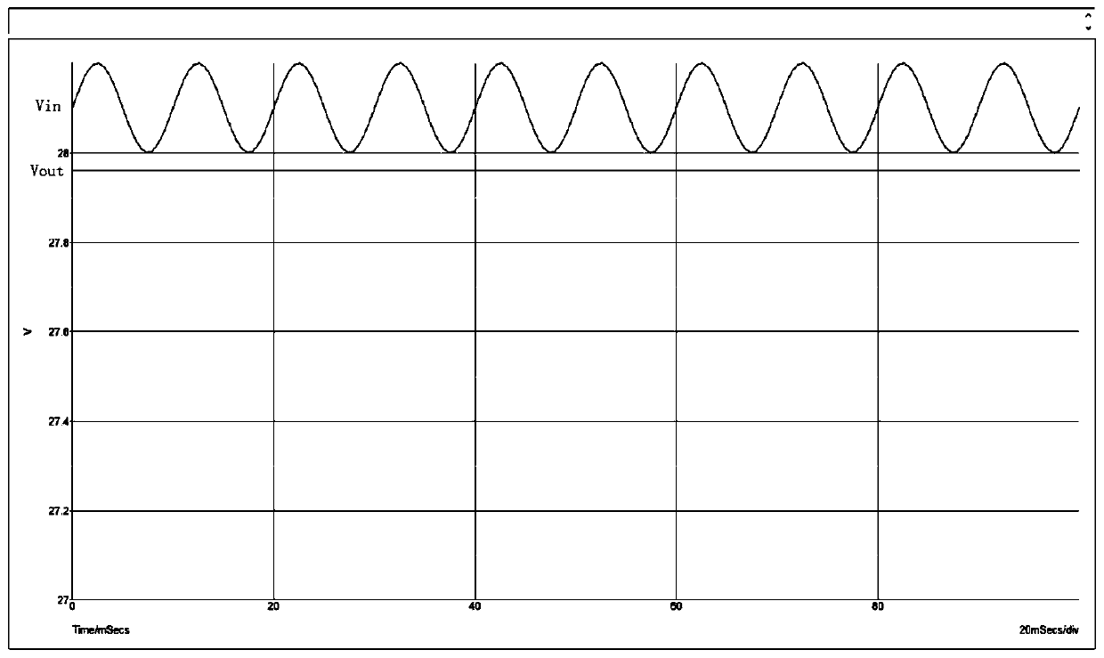
[0034] Such as figure 2 As shown, the basic implementation scheme of the present invention is a differential active follower filter, and the circuit is as figure 2 As shown, V1 and V2 form "input sampling Vin", resistor R3, resistor R5, and capacitor C2 form input sampling filter circuit 3, resistor R4, capacitor C3, and resistor R6 form output sampling circuit 4, and the output of operational amplifier X1 will follow the input The difference between output and input sampling filter circuit 3 and output sampling circuit 4 is used as follower circuit 5 and output to operational amplifier X2. Resistor R9 and Zener diode D2 are reference sources. Resistor R9, Zener diode D2 and operational amplifier X2, resistor R8 and capacitor C1 form a filtering and feedback control circuit 6 . The operational amplifier X2 adjusts the output of the operational amplifier X2 according to the output of the operational amplifier X1 and the reference source Vref, and controls the working state o...
Embodiment 2
[0051] Such as Figure 4 As shown, on the basis of the first embodiment, the follower circuit 5 and the filter and feedback control circuit 6 are composed of a follower, filter and feedback control unit, and the follower, filter and feedback control unit includes an operational amplifier X1 and a resistor R2, The power loop 7 includes a MOS transistor Q1, the positive input terminal of the operational amplifier X1 is connected to the output terminal of the output sampling circuit 2, and the negative input terminal of the operational amplifier X1 is connected to the output of the input sampling filter circuit 1 The output terminal of the operational amplifier X1 is connected to the gate of the MOS transistor Q1 through the resistor R2, the source of the MOS transistor Q1 is connected to the voltage input terminal 1, and the drain of the MOS transistor Q1 Pole connected to the voltage output terminal 2, the operational amplifier X1 adjusts its own output according to the differe...
Embodiment 3
[0073] Such as Figure 6 , 7 As shown, on the basis of Embodiment 1, a Zener diode D3 is added, specifically, the power supply follower filter circuit 6 further includes a Zener diode D3, and the anode of the Zener diode D3 is connected to the capacitor C2 and then grounded. The cathode of the Zener diode D3 is connected between the voltage input terminal 1 and the power loop 7 .
[0074] Zener diode D3 is to improve the response speed of the filter circuit when switching on and off. In addition, in some specific scenarios, in order to further improve the response speed of switching on and off of the active filter and the response speed of short-circuit protection, diode D4 will be added, such as Figure 6 , 7 shown.
[0075] The power loop 7 can use a P-MOSFET tube, an N-MOSFET tube, or a triode as the main device of the power loop. In the present invention, the diode D1 is used for protection of the power loop.
[0076] A power supply following filter circuit provided by...
PUM
 Abstract
Description
Claims
Application Information