A switch converter
A technology for switching converters and transformers, which is applied to instruments, converting DC power input to DC power output, adjusting electrical variables, etc., can solve problems such as unfavorable productization, high production costs, and many PCB layers, and reduce freewheeling. diode, lower turns ratio, lower cost effect
- Summary
- Abstract
- Description
- Claims
- Application Information
AI Technical Summary
Problems solved by technology
Method used
Image
Examples
no. 1 example
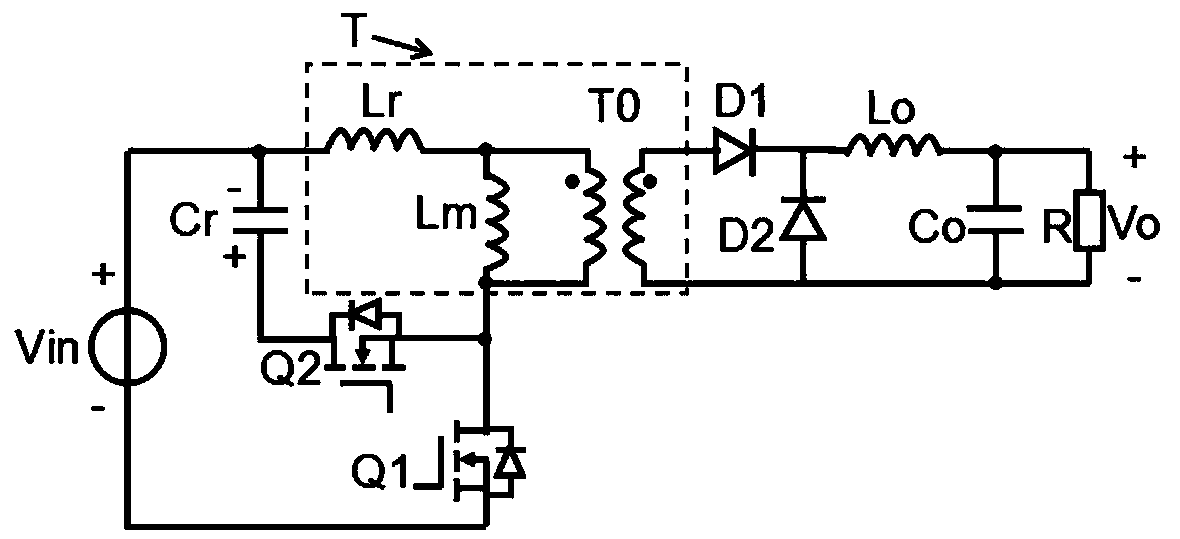
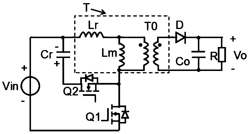
[0026] figure 2 It is a schematic diagram of the first embodiment of the switching converter power stage of the present invention. Among them, the voltage source Vin is the external input voltage, and the resistor R is the load of the switching power supply. The transformer of this invention includes capacitor Cr, MOS transistor Q1, MOS transistor Q2, transformer T, diode D and output capacitor Co. The dotted box in the figure is the equivalent schematic diagram of transformer T, which consists of leakage inductance Lr, excitation The inductance Lm and the ideal transformer T0 are composed. The leakage inductance Lr and the excitation inductance Lm are equivalent drawings, which appear in the figure for the convenience of description, and do not exist in the actual circuit.
[0027] The connection relationship of this embodiment is as follows:
[0028] The positive end of the voltage source Vin is respectively connected to the negative end of the capacitor Cr and the end of...
no. 2 example
[0038] Figure 5 It is one of the principle diagrams of the second embodiment of the switching converter power stage of the present invention.
[0039]On the basis of Embodiment 1, in order to increase the leakage inductance of the transformer T, an inductor L is externally connected outside the transformer T, and the connection relationship of the inductor L is one of the following four ways:
[0040] Method 1: The inductance L is connected between the negative terminal of the capacitor Cr and the terminal with the same name of the primary winding of the transformer T;
[0041] Method 2: The inductance L is connected between the source of the MOS transistor Q2 and the opposite end of the primary winding of the transformer T;
[0042] Method 3: The inductance L is connected between the same-named end of the secondary winding of the transformer T and the anode of the diode D;
[0043] Method 4: The inductor L is connected between the opposite end of the secondary winding of t...
no. 3 example
[0047] Figure 6 It is a schematic diagram of the third embodiment of the switching converter power stage of the present invention.
[0048] The positive end of the voltage source Vin is connected to the drain of the MOS transistor Q1, the source of the MOS transistor Q1 is respectively connected to the negative end of the capacitor Cr and the same name end of the primary winding of the transformer T, and the positive end of the capacitor Cr is connected to the drain of the MOS transistor Q2 The source of the MOS transistor Q2 is connected to the negative end of the voltage source Vin and the opposite end of the primary winding of the transformer T; the same end of the secondary winding of the transformer T is connected to the anode of the diode D, and the cathode of the diode D is connected to the output capacitor One end of Co is connected, the other end of the output capacitor Co is connected to the opposite end of the secondary side of the transformer T, one end of the out...
PUM
 Abstract
Description
Claims
Application Information
 - R&D
- Intellectual Property
- Life Sciences
- Materials
- Tech Scout
- Unparalleled Data Quality
- Higher Quality Content
- 60% Fewer Hallucinations
Browse by: Latest US Patents, China's latest patents, Technical Efficacy Thesaurus, Application Domain, Technology Topic, Popular Technical Reports.
© 2025 PatSnap. All rights reserved.Legal|Privacy policy|Modern Slavery Act Transparency Statement|Sitemap|About US| Contact US: help@patsnap.com


