

Medium-thick epitaxial preparation method
A thick epitaxy and epitaxy technology used in semiconductor/solid-state device manufacturing, discharge tubes, electrical components, etc.
- Summary
- Abstract
- Description
- Claims
- Application Information
AI Technical Summary
Problems solved by technology
Method used
Image

Examples
Embodiment 1
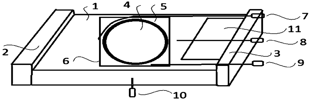
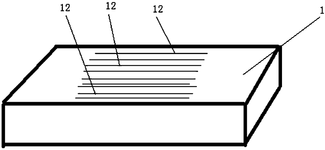
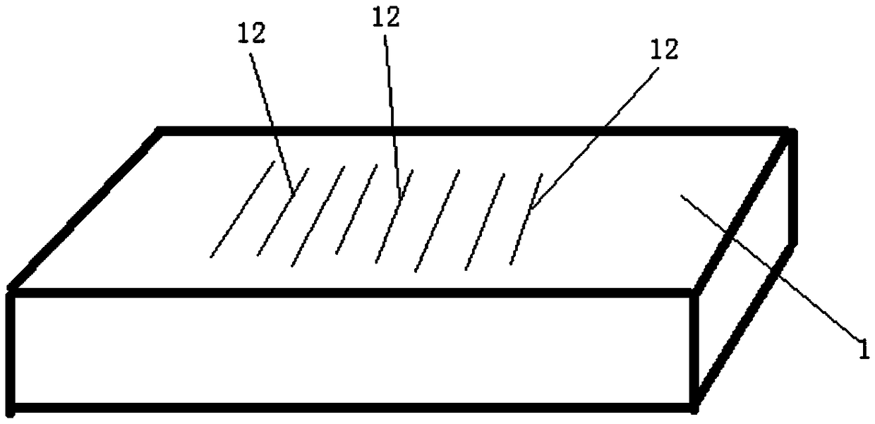
[0025] The preparation method of thick epitaxy in this embodiment includes the following steps: Step one, etching the cavity 1, wherein a heat absorption device is provided between the base of the cavity 1 and the air outlet,
[0026] Step a: First, perform a 15-second temperature increase to increase the temperature of the cavity 1 to 1120°C. During this process, 3 liters of hydrogen gas per minute is passed;
[0027] Step b. Then perform the first step of etching. The duration is 10 seconds, the temperature is maintained at 1120°C, the hydrogen is 3 liters / minute, and the hydrogen chloride is 15 liters / minute;
[0028] Step c. Then perform the second step of etching. The duration is 8*(T-4) seconds, and the duration is at least 15 seconds. T is the epitaxial thickness that needs to be grown on the silicon wafer in the cavity 1, such as a certain type of customer The product epitaxial thickness specification is 6 microns or 30 microns, T is correspondingly set to 6 or 30, the temper...
Embodiment 2
[0036] The preparation method of thick epitaxy in this embodiment includes the following steps: step one, etching the cavity 1, wherein a heat absorption device is provided between the base of the cavity 1 and the air outlet,
[0037] Step a: First, perform a temperature increase for 20 seconds to increase the temperature of the cavity 1 to 1170°C. During this process, 5 liters of hydrogen gas per minute is passed;
[0038] Step b. Then perform the first step of etching, which lasts for 15 seconds, maintains the temperature at 1170°C, blows 5 liters / min of hydrogen, and blows 20 liters / min of hydrogen chloride;
[0039] Step c. Then perform the second step of etching. The duration is 8*(T-2) seconds, and the duration is at least 20 seconds. T is the epitaxial thickness that needs to be grown on the silicon wafer in the cavity 1, and the temperature is maintained at 1170°C. 20 liters of hydrogen per minute and 20 liters of hydrogen chloride per minute;
[0040] The heat absorption devi...
Embodiment 3
[0052] The preparation method of thick epitaxy in this embodiment includes the following steps: step one, etching the cavity 1, wherein a heat absorption device is provided between the base of the cavity 1 and the air outlet,
[0053] Step a. First, perform a temperature increase of 17 seconds to increase the temperature of the cavity 1 to 1150°C. During this process, 4 liters of hydrogen gas per minute is passed;
[0054] Step b. Then perform the first step of etching, the duration is 12 seconds, the temperature is maintained at 1150°C, the hydrogen gas is 4 liters / min, and the hydrogen chloride is 17 liters / min;
[0055] Step c. Then perform the second step of etching. The duration is 8*T seconds and the duration is at least 18 seconds. T is the epitaxial thickness that needs to be grown on the silicon wafer in the cavity 1, the temperature is maintained at 1150°C, and the hydrogen gas is 18 liters / Minutes, and 18 liters of hydrogen chloride per minute;
[0056] The heat absorption...
PUM
| Property | Measurement | Unit |
|---|---|---|
| thickness | aaaaa | aaaaa |
| thickness | aaaaa | aaaaa |
| thickness | aaaaa | aaaaa |
Abstract
Description
Claims
Application Information