Semiconductor contact structure, memory structure and preparation method

A memory and semiconductor technology, applied in the fields of semiconductor/solid-state device manufacturing, semiconductor devices, electric solid-state devices, etc., can solve the problems affecting the structural performance of the memory, the consumption of the connection pad layer, and the small width of the connection part of the memory cell node.

Pending Publication Date: 2018-12-14
CHANGXIN MEMORY TECH INC
View PDF0 Cites 21 Cited by
  • Summary
  • Abstract
  • Description
  • Claims
  • Application Information

AI Technical Summary

Problems solved by technology

However, when etching the connection pad layer to form an opening in the connection pad layer to form the connection pad, due to the existence of etching by-products, or the opening is too small, or the opening Etching dislocation can easily lead to a short circuit connection between the adjacent connecting pads that are electrically connected to the storage unit node 1'; and in order to avoid the electrical connection between adjacent connecting pads, it is necessary to etch and remove enough The connection pad layer, so that the opening for

Method used


Image

  • Semiconductor contact structure, memory structure and preparation method
  • Semiconductor contact structure, memory structure and preparation method
  • Semiconductor contact structure, memory structure and preparation method

Examples


Embodiment 1

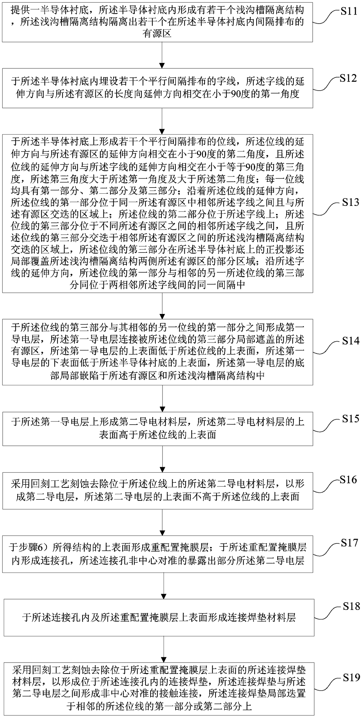
[0158] like figure 1 As shown, the present invention provides a method for preparing a memory structure, and the method for preparing the memory structure includes the following steps:

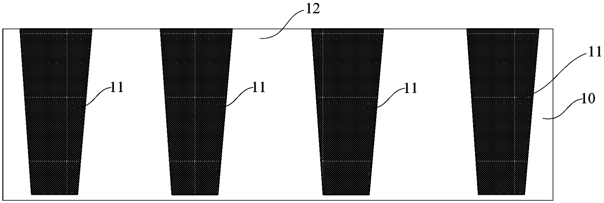
[0159] 1) A semiconductor substrate is provided, and several shallow trench isolation structures are formed in the semiconductor substrate, and the shallow trench isolation structures isolate several active regions arranged at intervals in the semiconductor substrate;

[0160] 2) Embedding several word lines arranged in parallel at intervals in the semiconductor substrate, the extending direction of the word lines intersects with the extending direction of the length of the active region at a first angle less than 90 degrees;

[0161] 3) forming a plurality of bit lines arranged in parallel at intervals on the semiconductor substrate, the extension direction of the bit lines intersects with the extension direction of the active region at a second angle less than 90 degrees, and the bit lines ...

Embodiment 2

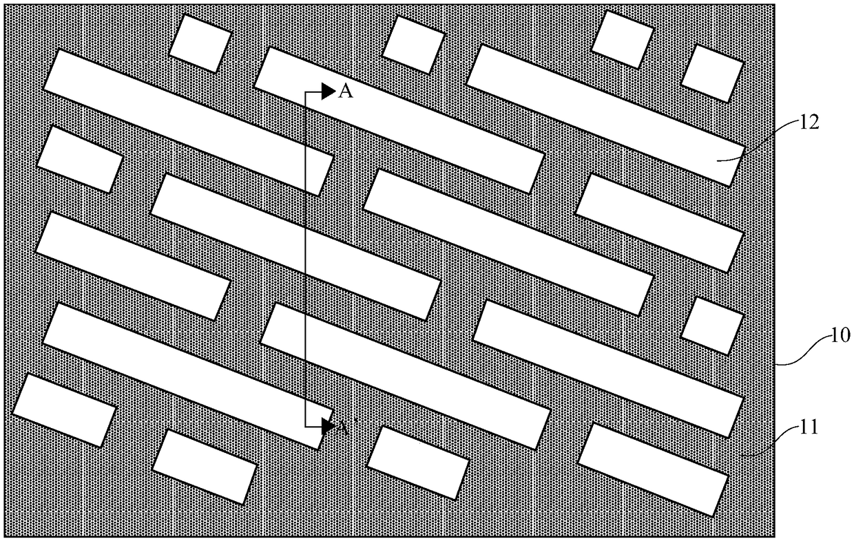
[0219] Please combine Figure 1 to Figure 20 read on Figure 22 , the present invention also provides a memory structure, the memory structure includes: a semiconductor substrate 10, the semiconductor substrate 10 is formed with several shallow trench isolation structures 11, and the shallow trench isolation structures 11 isolate several Active regions 12 arranged at intervals in the semiconductor substrate 10; several word lines 13 arranged in parallel at intervals, the word lines 13 are buried in the semiconductor substrate 10, and the extension of the word lines 13 The direction intersects the lengthwise extending direction of the active region 12 at a first angle α less than 90 degrees; several bit lines 14 arranged in parallel at intervals, the bit lines 14 are located on the semiconductor substrate 10, the The extending direction of the bit line 14 intersects with the extending direction of the active region 12 at a second angle β less than 90 degrees, and the extending...

Embodiment 3

[0238] see Figure 23 , the present invention also provides a method for preparing a semiconductor contact structure, the method for preparing a semiconductor contact structure includes the following steps:

[0239] 1) providing a semiconductor substrate, in which functional devices are formed;

[0240] 2) forming a contact hole in the semiconductor substrate, the contact hole exposing the functional device;

[0241] 3) forming a conductive material layer in the contact hole and on the surface of the semiconductor substrate;

[0242] 4) using an etch-back process to etch and remove the conductive material layer located on the surface of the semiconductor substrate to form a conductive layer located in the contact hole, the conductive layer is electrically connected to the functional device; the conductive plug The upper surface of is not higher than the upper surface of the semiconductor substrate;

[0243] 5) forming a reconfiguration mask layer on the upper surface of the...


PUM


Abstract

The invention provides a semiconductor contact structure, a memory structure and a preparation method thereof. The preparation method of the memory structure comprises the following steps: 1) providing a semiconductor substrate; 2) a plurality of word lines are formed at parallel intervals in that semiconductor substrate; 3) bury a plurality of bit lines arrange at parallel intervals on that semiconductor substrate; 4) for a first conductive layer on that bit line; 5) for a second conductive material layer on that first conductive lay; 6) etch that second conductive material layer to form a second conductive lay by adopting a back etching process; 7) for a reconfiguration mask layer on that upper surface of the structure obtain in the step 6); Forming connection holes in the reconfigured mask layer; 8) for a connection pad material layer in that connection via hole and on the upper surface of the reconfigured mask layer; 9) etching the connection pad material lay to form a connection pad by adopting a etching-back process. The invention can improve the contact resistance of the connection pad and the bridging tolerance between the connection pads.

Description

technical field [0001] The invention belongs to the technical field of semiconductor integrated circuit manufacturing, and in particular relates to a semiconductor contact structure, a memory structure and a preparation method thereof. Background technique [0002] As the manufacturing process of Dynamic Random Access Memory (DRAM for short: DRAM) becomes more and more refined, it becomes more and more difficult to make the pattern forming the basis of unit nodes in the chip, especially in order to make the basic tolerance of storage unit nodes and unit contact nodes Generally, connection pads are required, but this makes the contact resistance of the connection pads and the bridging tolerance between the connection pads more fragile. The main reason is that in the prior art, the storage unit node and the connection pad layer are generally formed by depositing the same conductive material layer, that is, the connection pad layer is formed at the same time as the storage unit...

Claims


Application Information

Patent Timeline
IPC IPC(8): H01L21/768H01L27/108
CPCH01L21/76897H10B12/00H10B12/01
Inventor 不公告发明人
Owner CHANGXIN MEMORY TECH INC
Why Eureka
Try Eureka