

An organic electroluminescent device
An electroluminescent device and luminescence technology, which is applied in the direction of electric solid-state devices, electrical components, semiconductor devices, etc., can solve the problems of low light extraction efficiency, achieve high luminous efficiency, improve external quantum efficiency, and improve light extraction efficiency Effect
- Summary
- Abstract
- Description
- Claims
- Application Information
AI Technical Summary
Problems solved by technology
Method used
Image

Examples
Embodiment 1
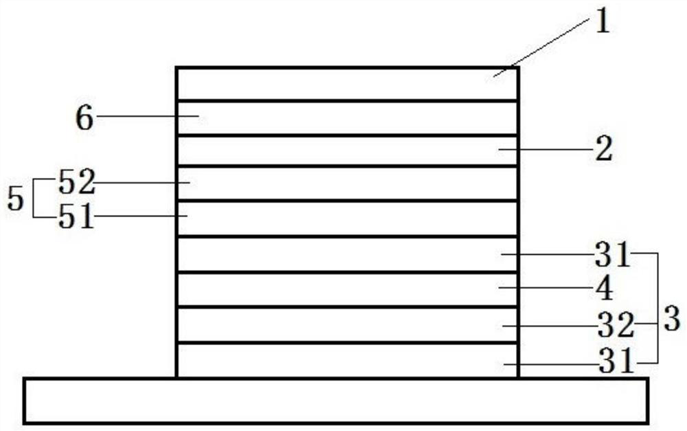
[0050] This embodiment provides an organic electroluminescent device, such as figure 1 As shown, it includes a reflective electrode layer 1 , a second carrier functional layer 6 , a light emitting layer 2 , a first carrier functional layer 5 and a reflective electrode layer 3 which are stacked sequentially from top to bottom. Wherein, the reflective electrode layer 3 includes a reflective metal layer 32 and a transparent electrode layer 31, the Bragg reflector layer 4 is arranged on the upper surface of the reflective metal layer 32, and the upper surface of the Bragg reflector layer 4 and the lower surface of the reflective metal layer 32 are respectively A transparent electrode layer 31 is provided.
[0051] The reflective electrode layer 1 is a translucent cathode layer, which is an alloy layer formed by mixing Mg and Ag at a mass ratio of 9:1.
[0052] The second carrier functional layer 6 is an electron transport layer, and the material of the electron transport layer is...
Embodiment 2
[0078] This embodiment provides an organic electroluminescence device, and the difference with the organic electroluminescence device in embodiment 1 is: the first reflector layer in the Bragg reflector layer 4 is SiNx (X takes 1-2) the thickness of SiNx d1=15nm, refractive index η1=1.9.
[0079] The above-mentioned organic light-emitting device complies with d*η=d1*η1+d2*η2+d3*η3+d4*η4+d5*η5=351 nm, therefore, the thickness d5 of the hole transport layer 52=(351-1.9*15- 1.5*50-2*20-1.9*5) / 1.9=104nm.
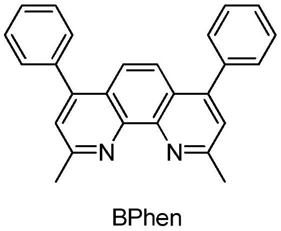
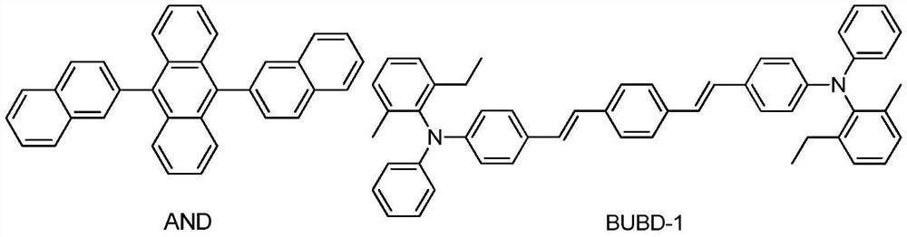
[0080] The organic electroluminescent device forms the following specific structure: ITO(20nm) / Ag(150nm) / SiNx(15nm) / SiO 2 (50nm) / ITO(20nm) / HAT(CN)6(5nm) / HTM081(104nm) / AND:5% BUBD-1(30nm) / Bphen(20nm) / Mg:Ag(9:1, 20nm).
Embodiment 3
[0082] This embodiment provides an organic electroluminescence device, and the difference with the organic electroluminescence device in embodiment 1 is: the first reflector layer in the Bragg reflector layer 4 is SiNx (X takes 1-2) the thickness of SiNx d1=15nm, refractive index η1=1.9; the second mirror layer in the Bragg mirror layer 4 is TiO 2 ,TiO 2 The thickness d2=50nm, the refractive index η2=2.2.
[0083] The above-mentioned organic light-emitting device complies with d*η=d1*η1+d2*η2+d3*η3+d4*η4+d5*η5=351 nm, therefore, the thickness d5 of the hole transport layer 52=(351-1.9*15- 2.2*50-2*20-1.9*5) / 1.9=86nm.
[0084] The organic electroluminescent device forms the following specific structure: ITO(20nm) / Ag(150nm) / SiNx(15nm) / TiO 2 (50nm) / ITO(20nm) / HAT(CN)6(5nm) / HTM081(86nm) / AND:5% BUBD-1(30nm) / Bphen(20nm) / Mg:Ag(9:1, 20nm).
PUM
| Property | Measurement | Unit |
|---|---|---|
| thickness | aaaaa | aaaaa |
| thickness | aaaaa | aaaaa |
| thickness | aaaaa | aaaaa |
Abstract
Description
Claims
Application Information