A packaging structure of an image sensor chip and a packaging method thereof

A technology of image sensing chip and packaging structure, which is applied in the direction of radiation control devices, electrical components, electric solid devices, etc., and can solve problems such as the influence of the image sensing area of ​​the image sensor chip

Pending Publication Date: 2018-12-18
CHINA WAFER LEVEL CSP
View PDF6 Cites 2 Cited by
  • Summary
  • Abstract
  • Description
  • Claims
  • Application Information

AI Technical Summary

Problems solved by technology

[0004] In order to solve the above-mentioned technical problems, the application provides a package structure of an image sensor chip and a package method thereof, so as to solve the problem that external moisture easily enters the airtight cavity through the package structure of the image sensor chip and affects the image of the image sensor chip. Problems with adverse effects in the sensing area

Method used


Image

  • A packaging structure of an image sensor chip and a packaging method thereof
  • A packaging structure of an image sensor chip and a packaging method thereof
  • A packaging structure of an image sensor chip and a packaging method thereof

Examples


Embodiment Construction

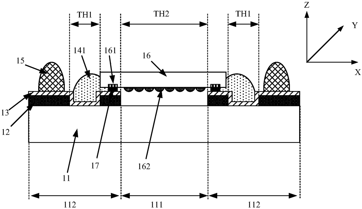
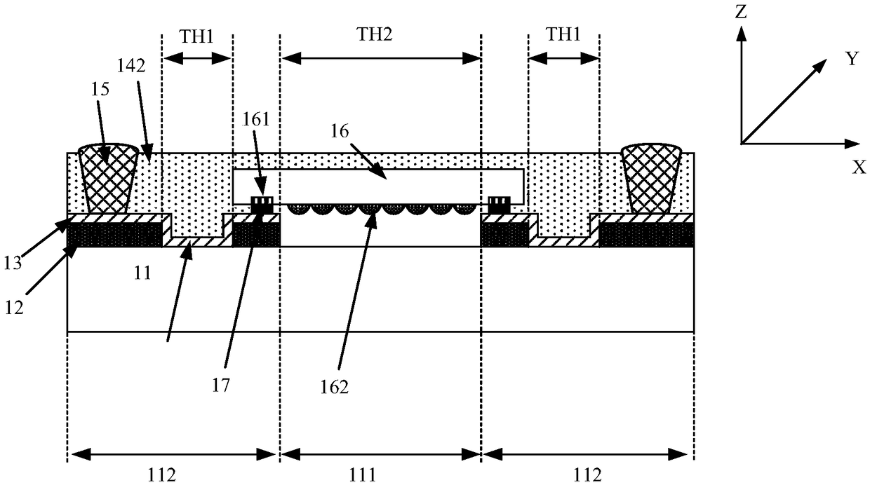
[0054] As mentioned in the background art, the packaging structure of the image sensor chip in the prior art is difficult to prevent external moisture from entering the airtight cavity, thereby adversely affecting the image sensing area of ​​the image sensor chip. The main reasons are as follows:

[0055]The base of the image sensor chip in the prior art is provided with a buffer layer, and the buffer layer is provided with a metal layer connected to the pad of the image sensor chip. connection, and finally form an airtight cavity structure between the image sensor chip and the substrate by arranging encapsulation layers on both sides of the image sensor chip. However, due to the strong hygroscopic performance of the materials used as the buffer layer, in this packaging structure, the external water vapor is easily absorbed by the buffer layer, and diffuses along the buffer layer into the closed cavity, thus making the waterproof and moisture-proof performance of the packaging...


PUM


Abstract

The invention discloses a packaging structure of an image sensing chip and a packaging method thereof, wherein the packaging structure of the image sensing chip passes through the packaging layer, thesubstrate and the image sensing chip form an airtight cavity for setting the image sensing area, and by providing a first groove in the buffer layer, direct contact of the buffer layer with the enclosed cavity is avoided, since the absorbent property of the buffer layer material is generally strong, isolating the buffer layer in contact with the outside from the enclosed cavity, External moisturecan be prevented from entering the enclosed space of the packaging structure of the image sensor chip through the buffer layer, thereby solving the problem that external moisture easily enters the enclosed cavity through the packaging structure of the image sensor chip and has adverse effects on the image sensing area of the image sensor chip.

Description

technical field [0001] The present application relates to the technical field of semiconductor packaging, and more specifically, relates to a packaging structure of an image sensor chip and a packaging method thereof. Background technique [0002] An image sensor chip is a sensor chip that senses external light and converts it into an electrical signal. After the image sensor chip is manufactured, a series of packaging processes are performed on the image sensor chip to form a packaged image sensor chip for use in various electronic devices such as digital cameras and digital video cameras. [0003] In the packaging structure of the image sensor chip, it is necessary to provide an airtight cavity for the image sensing area of ​​the image sensor chip, and provide good water and moisture-proof characteristics for the airtight cavity, so that the image sensing area of ​​the image sensor chip is free from Corroded by external water vapor. However, in the packaging structure in...

Claims


Application Information

Patent Timeline
Patent Type & Authority Applications(China)
IPC IPC(8): H01L27/146
CPCH01L27/14601H01L27/14683
Inventor 胡津津王之奇
Owner CHINA WAFER LEVEL CSP
Why Eureka
Try Eureka