A kind of ultra-thin wafer with reverse mesa composite structure and its preparation method

A composite structure and wafer technology, which is applied in semiconductor/solid-state device manufacturing, semiconductor/solid-state device components, semiconductor devices, etc., can solve problems such as surface finish decline, poor mechanical properties, rough surface structure, etc. Good use stability, not easy to be broken by force, and high surface finish

Active Publication Date: 2021-01-08
JINAN JINGZHENG ELECTRONICS
View PDF6 Cites 0 Cited by
  • Summary
  • Abstract
  • Description
  • Claims
  • Application Information

AI Technical Summary

Problems solved by technology

However, there is anisotropy in the chemical corrosion method, the surface finish of the corroded part decreases, and the equivalent resistance increases. In order to compensate for this shortcoming, it is necessary to increase the size of the electrode and increase the thickness of the electrode. Although the equivalent resistance is reduced, there are many parasitic , only suitable for ordinary resonators, not suitable for filters
Using the ion beam etching method, the surface finish of the etched part is high, the equivalent resistance of the crystal is small, and a smaller-sized electrode can be used, and the thickness of the electrode is thinner, and the parasitic can be made very small, but ion beam etching The corrosion method is inefficient and high in cost, which is not conducive to mass production
Therefore, the existing reverse mesa composite structure ultra-thin wafers have problems such as large thickness, poor mechanical properties, easy to break under force, rough surface structure, etc., which need to be solved urgently.

Method used


Image

  • A kind of ultra-thin wafer with reverse mesa composite structure and its preparation method
  • A kind of ultra-thin wafer with reverse mesa composite structure and its preparation method
  • A kind of ultra-thin wafer with reverse mesa composite structure and its preparation method

Examples


preparation example Construction

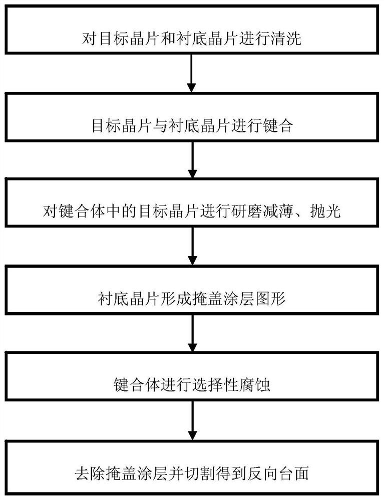
[0036] The present invention also includes a method for preparing an ultra-thin wafer with a reverse mesa composite structure, comprising the following steps:

[0037] ① Prepare the target wafer and the substrate wafer, clean and bond them respectively to obtain a bonded body; the target wafer is quartz, single crystal lithium tantalate, single crystal lithium niobate, silicon carbide or gallium arsenide; the substrate wafer is a silicon wafer, quartz wafer or glass wafer;

[0038] The prepared target wafer can be non-polished or a large-sized wafer (such as 3~6 inches) with single-sided and double-sided mirror polishing. The surface of the target wafer can be polished by chemical mechanical polishing. The surface roughness of the target wafer It is less than 1nm to meet the requirements of direct bonding; the target wafer can also be ground and thinned before polishing, and the TTV of the target wafer can be adjusted (thickness variation is less than 1 μm) to meet the thickne...

Embodiment 1

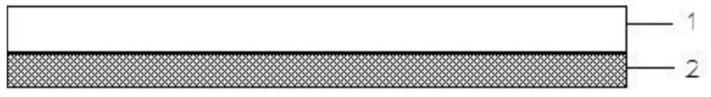
[0055] An ultra-thin wafer with a reverse mesa composite structure, including a target wafer and a substrate wafer positioned at the bottom of the target wafer with a supporting function, wherein the thickness of the target wafer is 2 μm, and a flat sheet with an overall thickness deviation of 0.005 to 1 μm, and the substrate wafer is frame structure; the target wafer is quartz; the substrate wafer is a silicon wafer.

Embodiment 2

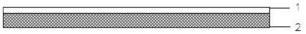
[0057] An ultra-thin wafer with a reverse mesa compound structure, including a target wafer and a substrate wafer at the bottom of the target wafer with a supporting function, wherein the target wafer is a flat sheet with a thickness of 80 μm and an overall thickness deviation of 0.005 to 1 μm, and the substrate wafer is frame structure; the target wafer is single crystal lithium tantalate; the substrate wafer is a quartz wafer.


PUM

PropertyMeasurementUnit
thicknessaaaaaaaaaa
surface roughnessaaaaaaaaaa
thicknessaaaaaaaaaa

Abstract

An ultra-thin wafer with reverse mesa composite structure and a preparation method thereof are disclosed, wherein the ultra-thin wafer includes a target wafer and a substrate wafer having a supportingfunction at the bottom of the target wafer, wherein the thickness of the target wafer is 2 to 80 [mu]m, a plate sheet with an overall thickness deviation of 0.005 to 1 [mu]m, The structure can not only effectively solve the problem that the ultra-thin wafer is easy to be broken due to its small thickness and poor mechanical properties, but also the substrate wafer is selectively etched to becomea frame structure without etching the target wafer, thus retaining its good surface structure and crystalline characteristics. According to the preparation method of the present application, the substrate wafer is protected by a mask coat, and a substrate wafer is selectively etched by an appropriate etching solution to obtain a reverse mesa composite structure. The preparation method of the present invention has no influence on the mechanical properties of a target wafer, has high surface finish, small thickness, can be industrialized and mass produced, and has high efficiency and low cost.

Description

technical field [0001] The invention relates to the technical field of semiconductors, in particular to an ultra-thin wafer with a reverse mesa compound structure and a preparation method thereof. Background technique [0002] Inverse mesa ultra-thin wafers are in great demand in some application fields, such as high-frequency quartz crystal oscillators, etc., and the device performance often has a decisive relationship with the thickness of the wafer. For example, quartz resonators need to use ultra-thin quartz wafers of 5-70 μm; high-sensitivity infrared pyroelectric sensors need to use ultra-thin lithium tantalate wafers of 5-60 μm; zero-order wave plates need to use 9-100 μm depending on the wave band quartz wafers, etc. However, during post-processing, packaging and use of ultra-thin chips, they are often easily broken due to small thickness and poor mechanical properties, which greatly affects the processing yield and stability of use. [0003] In order to improve th...

Claims


Application Information

Patent Timeline
Patent Type & Authority Patents(China)
IPC IPC(8): H01L23/13H01L21/48
CPCH01L21/48H01L23/13
Inventor 薛海蛟李洋洋胡文
Owner JINAN JINGZHENG ELECTRONICS
Why Eureka
Try Eureka