Resistive random access memory and preparation method thereof

A resistive variable memory and electrode layer technology, applied in the direction of electrical components, can solve the problems of unfavorable large-scale integration, low current density, small energy band gap, etc., to achieve three-dimensional integration, improve read efficiency, and reduce device size. area effect

Inactive Publication Date: 2018-12-21
INST OF MICROELECTRONICS CHINESE ACAD OF SCI
View PDF4 Cites 1 Cited by
  • Summary
  • Abstract
  • Description
  • Claims
  • Application Information

AI Technical Summary

Problems solved by technology

In the prior art, ferroelectric materials are mostly used in ferroelectric memory. In the integrated architecture of traditional ferroelectric memory, a transistor and a ferroelectric capacitor need to be integrated. This 1T1C structure is not conducive to large-scale integration and is destructive read
Moreover, traditional ferroelectric materials are not compatible with CMOS processes. For example, ferroelectric films with perovskite structures have ferroelectric size effects, small energy band gaps, and mismatches with silicon interfaces when applied to silicon-based ferroelectric devices. Problems such as performance degradation caused by heat treatment during the crystallization process
In addition, memories based on ferroelectric materials are generally thicker, resulting in lower current density, which limits the performance and miniaturization of devices.

Method used


Image

  • Resistive random access memory and preparation method thereof
  • Resistive random access memory and preparation method thereof
  • Resistive random access memory and preparation method thereof

Examples


preparation example Construction

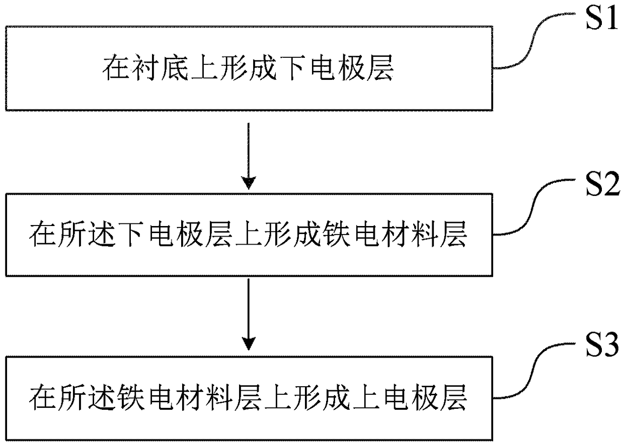
[0025] figure 2 shows the preparation figure 1 Flowchart of the method for the resistive variable memory. Such as figure 2 As shown, the preparation method of the resistive variable memory may include the following steps:

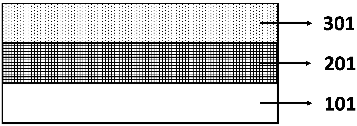
[0026] S1, forming a lower electrode layer 101 on the substrate;

[0027] S2, forming a ferroelectric material layer 201 on the lower electrode layer 101, the ferroelectric material layer 201 may include doped HfO 2 The ferroelectric thin film, specifically, the ferroelectric material layer 201 may include HfO doped with at least one element among Zr, Al, Si, La 2 Ferroelectric thin film;

[0028] S3, forming an upper electrode layer 301 on the ferroelectric material layer 201 .

[0029] Further, after the ferroelectric material layer 201 is formed on the lower electrode layer 101, an annealing treatment is performed, the annealing temperature is 400-1000°C, and the annealing time is 30-300s.

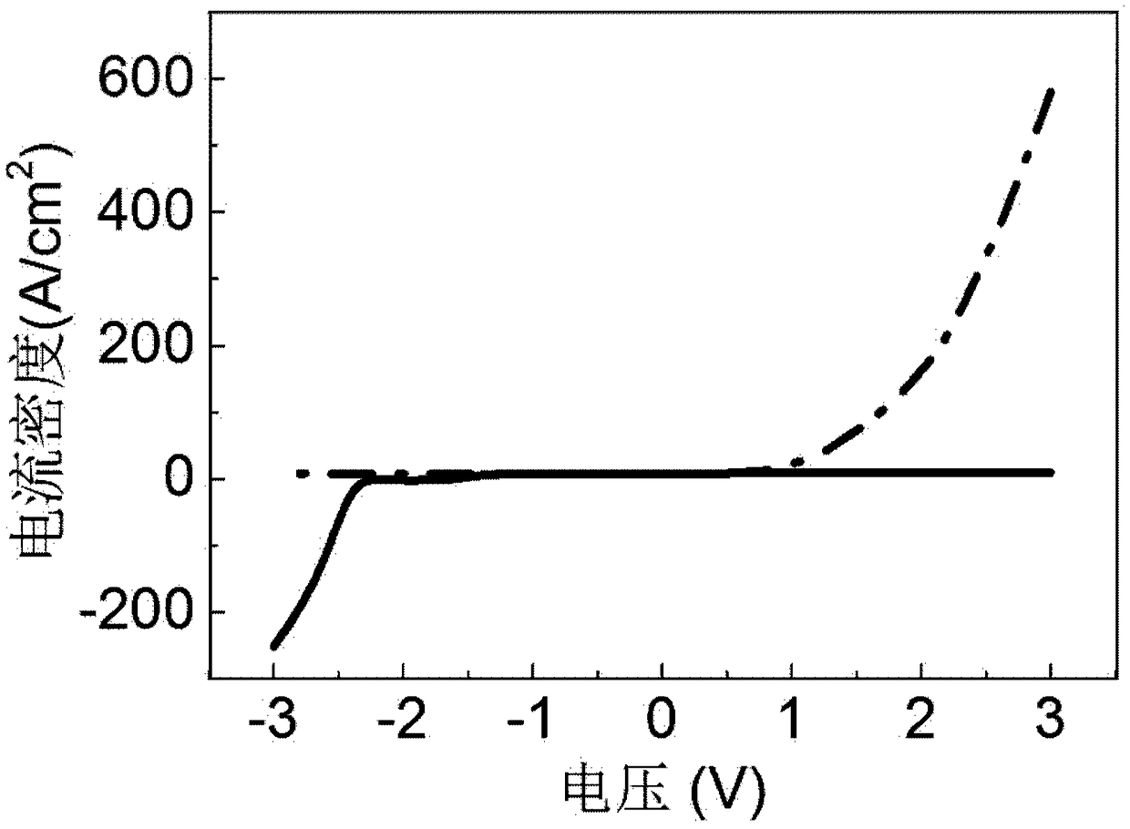
[0030] image 3 show figure 1 The current-voltage ch...

Embodiment 1

[0033] Preparation based on Hf 0.5 Zr 0.5 o 2 The resistive sensor with ferroelectric layer, the preparation process is as follows:

[0034] Step 1, adopting the sputtering method to form the TiN lower electrode layer, the process conditions are: power 25W~500W; pressure 0.1Pa~100Pa; Ar gas flow 0.5sccm~100sccm; the thickness of the obtained TiN lower electrode layer is 10nm~500nm;

[0035] Step 2: Cyclic growth of HfO on the TiN bottom electrode layer by ALD 2 and ZrO 2 to get Hf 0.5 Zr 0.5 o 2 For the ferroelectric layer, the process conditions are: power 25W~500W; pressure 0.1Pa~100Pa; gas flow 60sccm; temperature 250℃~300℃; rate about 0.07nm / cycle; growth cycle (cycle) HfO 2 followed by growing a cycle of ZrO 2 , reciprocating in this way, the two materials are mixed and deposited at a molar ratio of 1:1;

[0036] Step 3, performing annealing treatment, the annealing temperature is 400°C, and the annealing time is 30s;

[0037] Step 4, using the method of sputter...


PUM

PropertyMeasurementUnit
thicknessaaaaaaaaaa
thicknessaaaaaaaaaa

Abstract

The invention discloses a resistive memory, which is characterized in that the resistive memory comprises a lower electrode layer, a ferroelectric material layer and an upper electrode layer in orderfrom bottom to top, wherein the ferroelectric material layer comprises a doped HfO2 ferroelectric thin film.

Description

technical field [0001] Embodiments of the present invention relate to the technical fields of microelectronics manufacturing and memory, in particular to a resistive variable memory and a preparation method thereof. Background technique [0002] Ferroelectric materials are widely used in the fields of microelectronics manufacturing and memory technology. In the prior art, ferroelectric materials are mostly used in ferroelectric memory. In the integrated architecture of traditional ferroelectric memory, a transistor and a ferroelectric capacitor need to be integrated. This 1T1C structure is not conducive to large-scale integration and is destructive read. Moreover, traditional ferroelectric materials are not compatible with CMOS processes. For example, ferroelectric films with perovskite structures have ferroelectric size effects, small energy band gaps, and mismatches with silicon interfaces when applied to silicon-based ferroelectric devices. Problems such as performance ...

Claims


Application Information

Patent Timeline
Patent Type & Authority Applications(China)
IPC IPC(8): H01L45/00
CPCH10N70/041H10N70/8833
Inventor 罗庆吕杭炳刘明许晓欣路程赵盛杰
Owner INST OF MICROELECTRONICS CHINESE ACAD OF SCI
Why Eureka
Try Eureka