Wafer defect inspection and review systems
An inspection system and detector technology, applied in the inspection field, can solve the problem of inefficient and effective detection of inspection tools
- Summary
- Abstract
- Description
- Claims
- Application Information
AI Technical Summary
Problems solved by technology
Method used
Image

Examples
Embodiment Construction
[0018] Reference will now be made in detail to the disclosed subject matter, which is illustrated in the accompanying drawings.
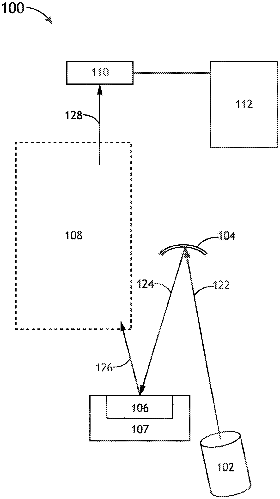
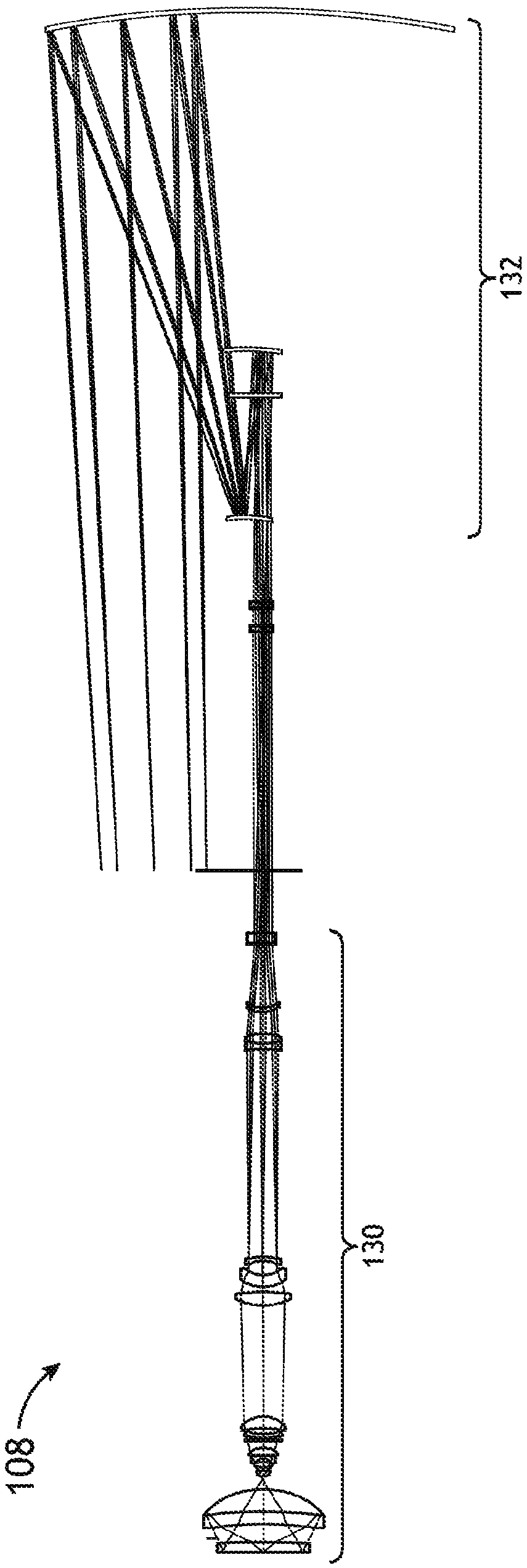
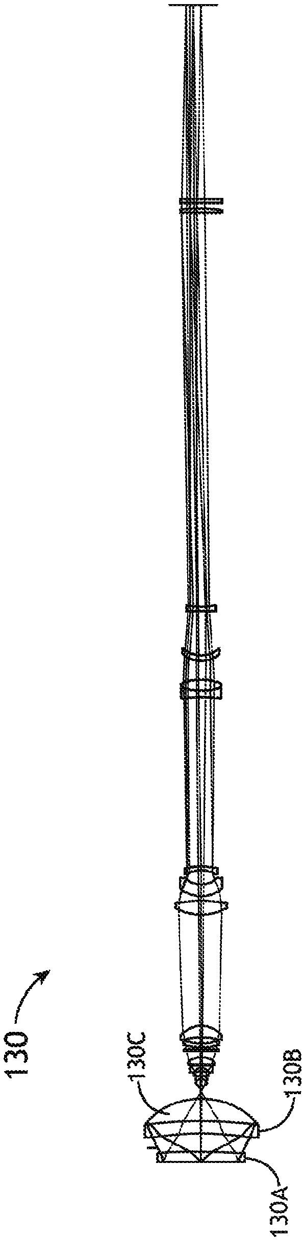
[0019] Embodiments according to the invention relate to imaging objectives and inspection systems equipped with such imaging objectives. Imaging objectives configured according to the invention can be characterized by perfect (eg, diffraction-limited) or imperfect intermediate images and three-mirror total reflection repeaters. An imaging objective configured in this manner may serve as a replacement for the imaging objective described in US Patent No. 6,894,834, which is hereby incorporated by reference in its entirety. It should be noted that the imaging objective described in US Patent No. 6,894,834 does not provide diffraction-limited performance at the intermediate image plane, making it unusable for confocal applications. It is contemplated that imaging objectives configured in accordance with embodiments of the present invention may be used ...
PUM
 Abstract
Description
Claims
Application Information
 - R&D
- Intellectual Property
- Life Sciences
- Materials
- Tech Scout
- Unparalleled Data Quality
- Higher Quality Content
- 60% Fewer Hallucinations
Browse by: Latest US Patents, China's latest patents, Technical Efficacy Thesaurus, Application Domain, Technology Topic, Popular Technical Reports.
© 2025 PatSnap. All rights reserved.Legal|Privacy policy|Modern Slavery Act Transparency Statement|Sitemap|About US| Contact US: help@patsnap.com