Supercharge Your Innovation With Domain-Expert AI Agents!

Package circuit system structure

A technology of system structure and packaging circuit, which is applied in the field of packaging circuit system and manufacturing packaged circuit system including two or more circuit elements, to achieve the effect of easy manufacture

Active Publication Date: 2022-04-05
MURATA MFG CO LTD
View PDF3 Cites 0 Cited by
  • Summary
  • Abstract
  • Description
  • Claims
  • Application Information

AI Technical Summary

Problems solved by technology

However, established leadless packaging technologies have not yet provided an adequate solution for EMI shielding under challenging conditions—typical in automotive applications

Method used


Image

  • Package circuit system structure
  • Package circuit system structure
  • Package circuit system structure

Examples


Embodiment Construction

[0017] The following embodiments are exemplary. Although the specification may refer to "a," "an," or "some" implementations, this does not necessarily mean that each such reference is to the same implementation, or that features are only applicable to a single implementation. Single features of different embodiments can be combined to provide further embodiments.

[0018] In the following, the features of the invention will be described using simple examples of device architectures in which various embodiments of the invention can be implemented. Only elements relevant to the illustrated embodiment have been described in detail. Various components of the integrated device that are generally known to those skilled in the art may not be specifically described herein.

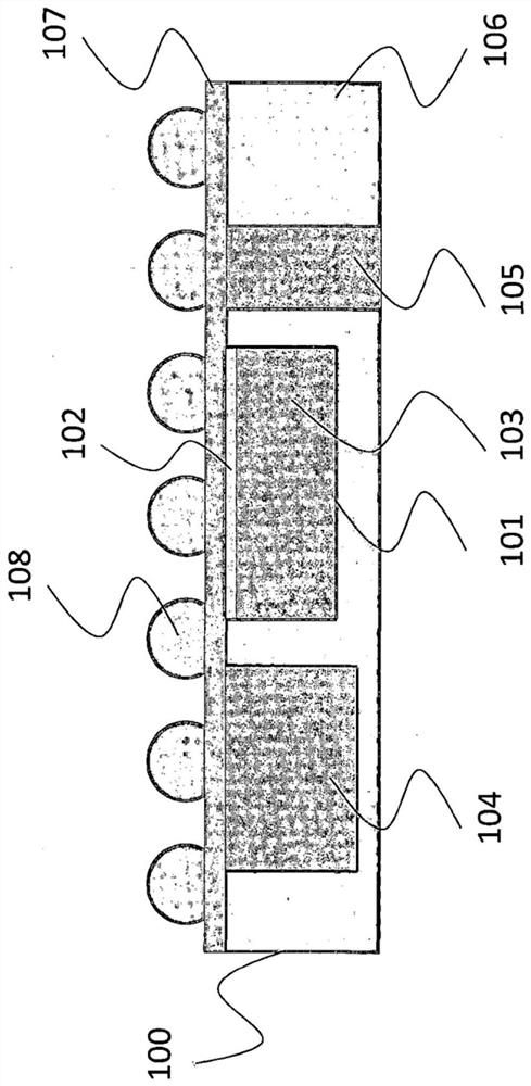
[0019] figure 1 A schematic diagram showing a typical prior art packaged circuit system structure. A structure includes one or more circuit elements (die), possibly of different origin (different wafer, desig...


PUM


Abstract

A packaged circuitry structure having circuit elements (301, 304) embedded in a bulk material (322). At least one of the embedded circuit elements (301, 304) forms an electrical connection that includes an electrical connection to a signal ground potential (350) on one side (324) of the structure and an electrical connection to a conductive layer (316) on the other side of the structure Double coupling. A conductive layer extends over at least one embedded circuit element (304) that does not form a double coupling, thereby providing effective EMI shielding therefor.

Description

technical field [0001] The present disclosure relates to circuitry, and more particularly to packaged circuitry that includes two or more circuit elements. The present disclosure also relates to methods for fabricating packaged circuitry including two or more circuit elements. Background technique [0002] Electromagnetic (EM) fields are defined as properties of space caused by the motion of charges (Encyclopedia Britannica). A charge at rest generates an electric field in the surrounding space, and when the charge is moving, a magnetic field is also generated. Electric fields can also be generated by changing magnetic fields. The interaction of electric and magnetic fields produces an electromagnetic field. [0003] Man-made and natural sources of electromagnetic fields in space can interfere with the operation of electrical equipment. For example, sensors used in automotive systems are exposed to varying fields and need to be effectively shielded from electromagnetic i...

Claims


Application Information

Patent Timeline
Patent Type & Authority Patents(China)
IPC IPC(8): H01L23/552H01L21/60B81C1/00
CPCB81B7/0064H01L23/5389H01L23/552H01L24/20H01L24/96H01L24/97H01L25/00H01L25/0655H01L2224/12105H01L2224/73267H01L2924/14H01L2924/1461H01L2924/18162H01L2924/19105H01L2924/30105H01L2924/3011H01L2924/3025H01L2924/30101H01L23/49816B81C1/00261H01L2225/06582H01L2225/06517H01L2225/06537H01L2225/06586H01L2225/0652
Inventor 海基·库斯玛
Owner MURATA MFG CO LTD
Features
  • R&D
  • Intellectual Property
  • Life Sciences
  • Materials
  • Tech Scout
  • Unparalleled Data Quality
  • Higher Quality Content
  • 60% Fewer Hallucinations
Learn More