Method for peeling off flexible substrate and display panel

A flexible substrate and backplane technology, applied in the direction of electrical components, electrical solid devices, circuits, etc., can solve the problems of low success rate, damage to the entire flexible OLED display panel, scratches or even punctures.

Inactive Publication Date: 2018-12-25
WUHAN CHINA STAR OPTOELECTRONICS SEMICON DISPLAY TECH CO LTD
5 Cites 7 Cited by

AI-Extracted Technical Summary

Problems solved by technology

However, if the flexible OLED display device uses this method, since the hardness of the flexible substrate 22' is very low, it is very easy to be scratched or even pierced by a knife (Knife) 29, thereby damaging the array layer 24' and the OLED layer 25'. During the opening process, the adhesive force between the rigid liner 28' and the flexible liner 22' is about 500Kg/inch 2 , far greater than the tearing force 10Kg/inch that the flexible OLED display panel 20' can bear 2 Therefore, in the process of...

Method used

[0082] The present invention provides a method for peeling off a flexible substrate and a display panel. In the above-mentioned embodiment, on the basis of the existing flexible display panel structure, the general optical adhesive layer (such as the first adhesive of the present invention) Layer) and then set a second adhesive layer, and bonded between the backplane and the flexible substrate, so that the flexible substrate is attached to the backplane, not only does not need to greatly change the preparation method of the original overall structure, but also It is not easy to be polluted and damaged during the subsequent heavy work; in addition, in the above-mentioned separation heavy work process, the adhesive film layer on the flexible substrate to be attached to the backplane is irradiated with 308nm laser to make it carbonized and Loss of adhesive performance, so that the backplane can be easily peeled of...

Abstract

The present invention discloses a peeling method of a flexible substrate and a display panel. The adhesive film layer is provided with two layers, one is a first adhesive layer including an optical adhesive, and the other is a second adhesive layer including an optical adhesive (OCA) and a yellow polyimide (PI) doped in the optical adhesive. By using the high absorbance of the second adhesive layer and the transmittance characteristic of 308 nm laser, As the 308 nm laser passes through the backplate, the 308 nm laser energy is absorbed by the second adhesive layer to form an extremely high temperature, resulting in failure of the first adhesive lay and carbonization of the second adhesive layer, thereby carbonizing the adhesive film layer. After the adhesive film is carbonized, the back plate can be easily separated from the flexible substrate, so as to achieve the purpose of smooth rework, and at the same time, the flexible display panel can not be damaged, thereby reducing the scraprate of the defective products and greatly reducing the production cost.

Application Domain

Solid-state devicesSemiconductor/solid-state device manufacturing +1

Technology Topic

PhysicsTransmittance +7

Image

  • Method for peeling off flexible substrate and display panel
  • Method for peeling off flexible substrate and display panel
  • Method for peeling off flexible substrate and display panel

Examples

  • Experimental program(1)

Example Embodiment

[0049] Please refer to the drawings in the drawings, in which the same component symbols represent the same components. The following structural drawings and description of the embodiments are based on the illustrated specific embodiments of the present invention. It should be understood that the specific embodiments described herein are only used to explain the present invention, and should not be regarded as limiting other specific embodiments of the present invention that are not described in detail herein.
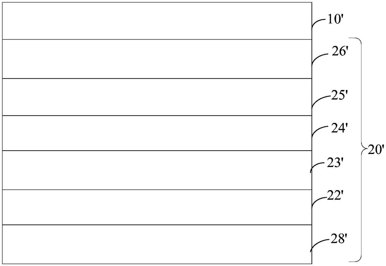
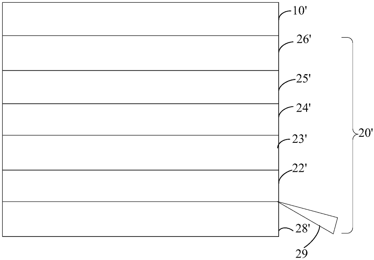
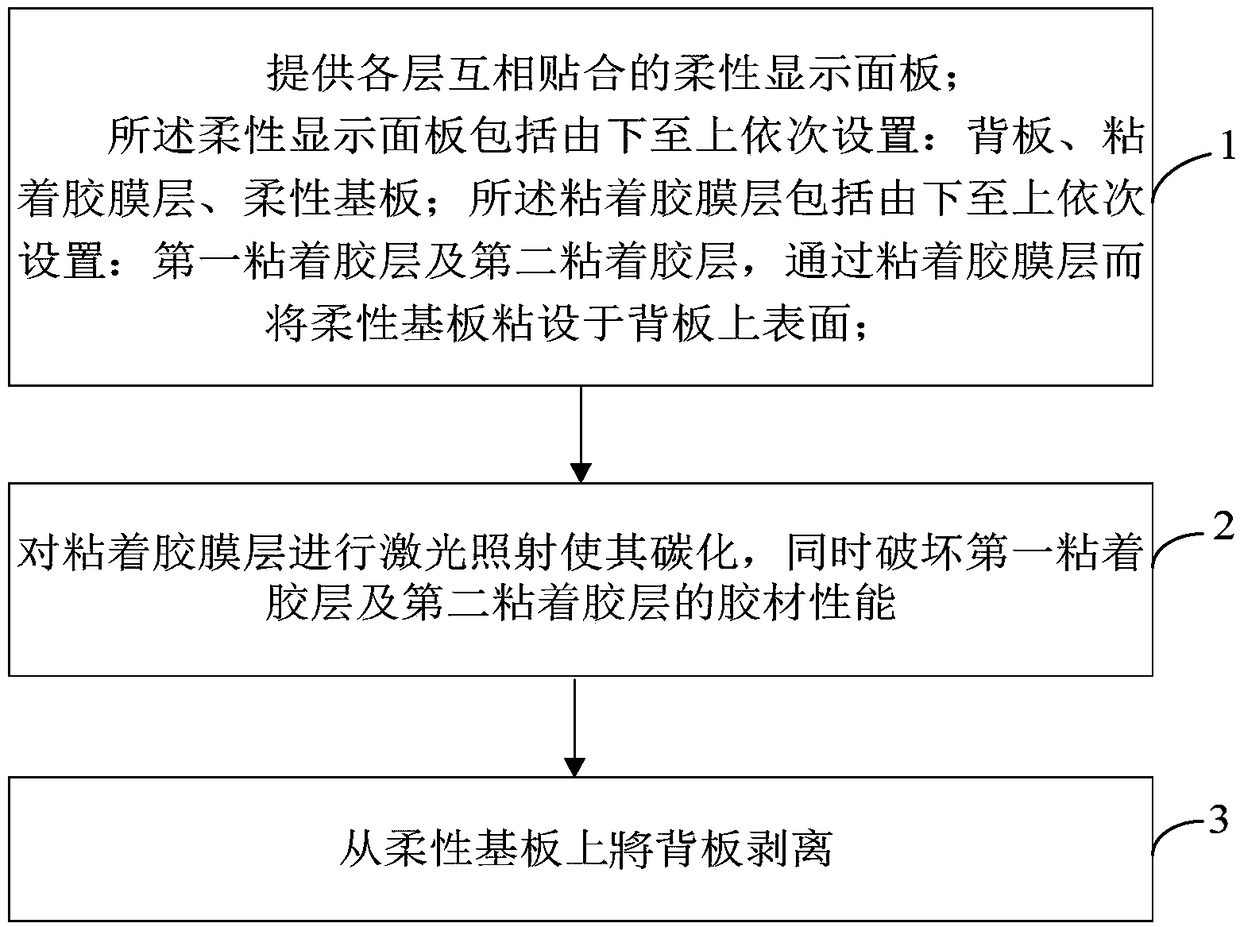
[0050] image 3 It is a flowchart of an embodiment of the peeling method of the flexible substrate of the present invention; Figure 4-5 It is a schematic diagram of step 2 of the peeling method of performing laser irradiation on the adhesive film layer to carbonize the backplane and the flexible substrate according to the present invention.
[0051] See image 3 In a preferred embodiment, the method for peeling off a flexible substrate of the present invention includes the following steps:
[0052] Step 1, please refer to Figure 4 , Provide a flexible display panel 20 in which the layers are attached to each other.
[0053] In a preferred embodiment, the flexible display panel 20 includes a backplane 21, an adhesive film layer 27, and a flexible substrate 30 arranged in order from bottom to top. The flexible substrate 30 includes a flexible substrate 301, a buffer layer 302, an array layer 303, an OLED layer 304, and a touch sensing layer 305; this is only an example, and may also include other components, such as a polarizing component. Limitations.
[0054] Specifically, the adhesive film layer 27 includes a first adhesive layer 271 and a second adhesive layer 272 arranged in order from bottom to top. The flexible substrate 30 is adhered to the upper surface of the back plate 21 through the adhesive film layer 27. .
[0055] Step 2: Perform laser irradiation on the adhesive film layer 27 to carbonize it, and at the same time destroy the adhesive properties of the first adhesive layer 271 and the second adhesive layer 272.
[0056] Specifically, the material of the first adhesive layer 271 includes optical glue.
[0057] Specifically, the material of the second adhesive layer 272 includes optical adhesive (OCA) and yellow polyimide (PI) doped in the optical adhesive. The yellow polyimide (PI) has excellent laser high temperature absorption. The effectiveness of.
[0058] Specifically, the optical glue is used to fail under laser irradiation, and the yellow polyimide (PI) is an absorbing part for absorbing laser light.
[0059] It should be noted that after the adhesive film layer 27 is carbonized by laser irradiation, the optical adhesives of the first and second adhesive layers 271 and 272 will lose their adhesion, and the yellow polyimide (PI) will fail, causing the flexible substrate on it. 30 is no longer attached to the upper surface of the back plate 21.
[0060] Step 3: Peel the back plate 21 from the flexible substrate 30.
[0061] It should be noted that after step 2 is completed, the upper surface of the flexible substrate 30 and the back plate 21 is no longer attached (because the adhesive film layer 27 is carbonized), so in step 3, a small external force can be used The back plate 21 is peeled from the flexible substrate 30, leaving only the flexible substrate 30. So far, the separation of the backplane 21 and the flexible substrate 30 is completed.
[0062] In another preferred embodiment, the flexible display panel in step 1 includes the backplane 21, the adhesive 27', and the flexible substrate 30 arranged in order from bottom to top. The adhesive 27' includes:
[0063] The first adhesive layer, including the adhesive part; and
[0064] The second adhesive layer is provided on the upper surface of the first adhesive layer. The second adhesive layer includes a sticking part and an absorbing part. The absorbing part is used for absorbing laser light. Failure under the exposure.
[0065] Specifically, the absorbing part of the second adhesive layer is doped in the sticking part.
[0066] Specifically, the sticking part of the second adhesive layer includes optical adhesive (OCA), and the absorbing part is yellow polyimide (PI).
[0067] Preferably, the material of the back plate 21 is PET.
[0068] Preferably, the material of the flexible substrate 301 is polyimide.
[0069] Preferably, the array layer 303 is formed by a TFT array or other arrays.
[0070] Preferably, the laser is a 308nm laser.
[0071] Specifically, see Figure 4 to Figure 6 , The step 2 is specifically: the material of the second adhesive layer 272 includes optical adhesive (OCA) and yellow polyimide (PI) doped in the optical adhesive, because the yellow PI (polyimide) pairs The absorption rate of the laser (the 308nm laser) is relatively high, reaching an efficiency of over 99.6%; and the penetration rate of the 308nm laser to the back plate and the first adhesive layer is about 90%. Therefore, when the 308nm laser irradiates the backplane and the adhesive film layer, when the 308nm laser passes through the backplane, most of the laser energy is absorbed by the structure of the second adhesive layer, thus causing the second adhesive layer The temperature of the structure is extremely high. This extremely high temperature will cause most of the performance of the first and second adhesive layers (ie optical adhesive materials) to fail. At the same time, the laser will also carbonize the second adhesive layer structure, that is, destroy both at the same time. The performance of the adhesive material makes the first adhesive layer and the second adhesive layer carbonized, and further makes the back plate adhered to the first adhesive layer very easy to contact with the flexible lining adhered to the second adhesive layer The board is separated, so as to achieve the purpose of subsequent smooth rework without causing damage to the flexible substrate 30.
[0072] Specifically, see Figure 4 and Figure 5 , The step 2 specifically includes: irradiating the back plate and the adhesive film layer with a 308nm laser beam from one side of the surface of the back plate 21 and the adhesive film layer 27 to the opposite side, so that the adhesive film layer Carbonization.
[0073] The peeling method of the flexible substrate described above further includes: step 4, cleaning the carbonized adhesive film layer on the flexible liner. Specifically, isopropanol solvent or other solvents can be used to easily dissolve the carbonized adhesive film layer, so as to clean the carbonized adhesive film layer on the flexible substrate to improve the quality of peeling the flexible substrate.
[0074] In order to solve the above technical problems, another technical solution adopted by the present invention is to provide a display panel, which can be manufactured by applying any of the above methods. In a preferred embodiment, the display panel includes:
[0075] Flexible substrate with luminous front surface;
[0076] The adhesive film layer is irradiated by the laser to carbonize according to the above method, and at the same time destroy the adhesive properties of the first adhesive layer and the second adhesive layer, lose effectiveness and be removed;
[0077] The backplane can be separated from the flexible substrate.
[0078] Specifically, in the above display panel, the adhesive film layer includes the following steps:
[0079] The first adhesive layer, including a general optical adhesive layer, is arranged on the upper surface of the back plate; and
[0080] The second adhesive layer includes an optical adhesive (OCA) and yellow polyimide (PI) doped in the optical adhesive. The yellow polyimide (PI) has an excellent function of absorbing high temperatures. The second adhesive layer is arranged on the upper surface of the first adhesive layer, and the flexible liner is adhered to the upper surface of the back plate through the adhesive film layer (including the second adhesive layer and the first adhesive layer).
[0081] In a preferred embodiment, in the above-mentioned flexible display panel, the flexible substrate includes a flexible substrate, a buffer layer, an array layer, an OLED layer, and a touch sensing layer arranged in order from bottom to top. This is only an example, and other components may be included without limitation.
[0082] The present invention provides a method for peeling off a flexible substrate and a display panel. In the above-mentioned embodiments, on the basis of the existing flexible display panel structure, a general optical adhesive layer (such as the first adhesive layer of the present invention) can be used. A second adhesive layer is then arranged and glued between the backplane and the flexible substrate, so that the flexible substrate is attached to the backplane, not only does not need to greatly change the original overall structure preparation method, but also continues to follow It is not easy to be damaged by pollution during the heavy-duty operation; in addition, during the above-mentioned separation and heavy-duty operation process, the adhesive film layer of the flexible substrate to be attached to the backplane is irradiated with 308nm laser to carbonize and lose the adhesive performance , So that the backplane can be easily peeled off from the flexible substrate, and then the carbonized adhesive film layer on the flexible substrate can be cleaned. There is no need to use large external force or a knife to tear and separate the backplane and the flexible substrate. The separation operation has a high success rate, and it can also effectively prevent the flexible substrate itself or the various layer structures of the flexible substrate from being torn apart by external forces during the separation process, resulting in damage to the flexible substrate itself, or between the various layer structures of the flexible substrate. Poor peeling results in a very low separation success rate, so that subsequent rework operations cannot be carried out, which effectively improves the use breadth and efficiency of separation rework operations, thereby reducing the rejection rate of defective products and greatly reducing production costs.
[0083] In summary, although the present invention has been disclosed in preferred embodiments as described above, the above descriptions are only implementations of the present invention and do not therefore limit the scope of the present invention. Those of ordinary skill in the art will not depart from the present invention. Various changes and modifications can be made within the spirit and scope. Any equivalent structure or equivalent process transformation made using the contents of the description and drawings of the present invention, or directly or indirectly applied to other related technical fields, is the same. It is included in the scope of patent protection of the present invention.

PUM

no PUM

Description & Claims & Application Information

We can also present the details of the Description, Claims and Application information to help users get a comprehensive understanding of the technical details of the patent, such as background art, summary of invention, brief description of drawings, description of embodiments, and other original content. On the other hand, users can also determine the specific scope of protection of the technology through the list of claims; as well as understand the changes in the life cycle of the technology with the presentation of the patent timeline. Login to view more.
Why Eureka
Try Eureka