Circuit of radio frequency amplifier

A technology of amplifier circuits and resistors, applied in the field of signal processing, can solve problems such as useless amplifier circuits, achieve low power consumption, good current use efficiency, and meet stringent requirements

Pending Publication Date: 2018-12-25
安徽矽磊电子科技有限公司
View PDF0 Cites 1 Cited by
  • Summary
  • Abstract
  • Description
  • Claims
  • Application Information

AI Technical Summary

Problems solved by technology

[0007] It can be seen from the above that in order to ensure the accurate DC operating current of the amplifier, the existing amplifier circuit needs an additional part of the current to ensure t

Method used


Image

  • Circuit of radio frequency amplifier
  • Circuit of radio frequency amplifier

Examples


Embodiment Construction

[0018] In order to make the objectives, technical solutions, and advantages of the present invention clearer, the embodiments of the present invention will be described in detail below with reference to the accompanying drawings. It should be noted that the embodiments in the application and the features in the embodiments can be combined with each other arbitrarily if there is no conflict.

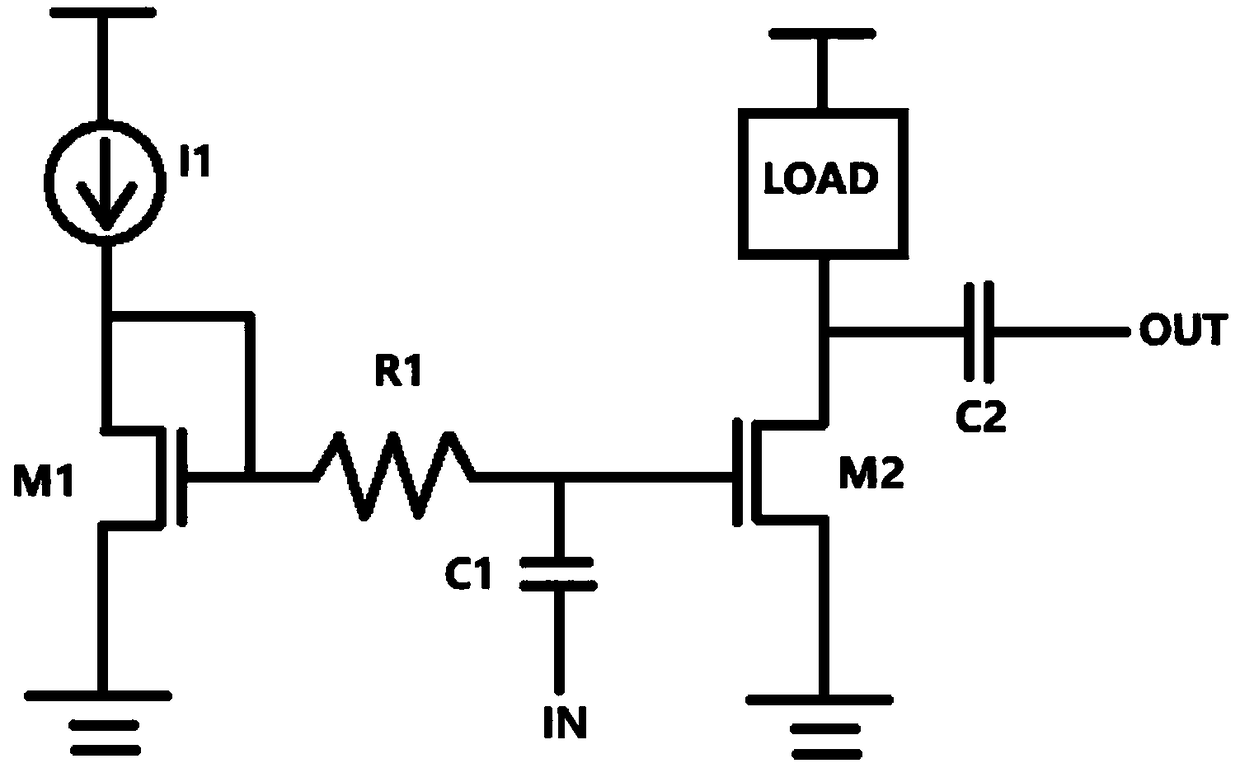
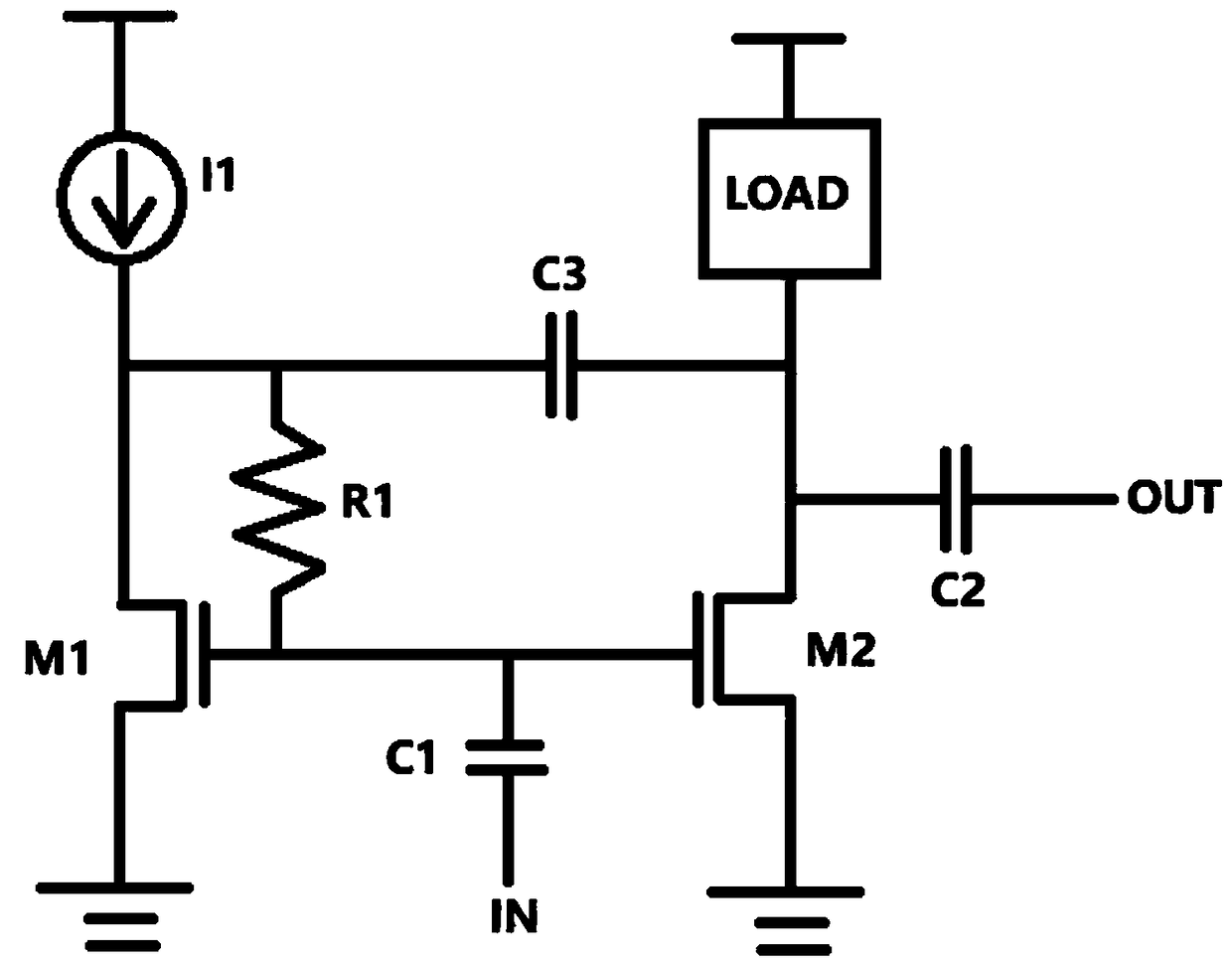
[0019] In order to further improve the current usage efficiency of the existing amplifier, the embodiment of the present invention provides an improved radio frequency amplifier structure and its bias circuit. The specific circuit diagram is as follows figure 2 Shown. Among them, the amplifier is composed of capacitor C1, capacitor C2, capacitor C3, N-type CMOS transistors M1 and M2, resistor R1, and load part LOAD. One end of the capacitor C1 is connected to the signal input end (such as the radio frequency signal input end), and the other end is connected to the gates of the transistors ...


PUM


Abstract

The invention provides an amplifier circuit, which is composed of a first capacitor, a first transistor, a second transistor, a first resistor, a current source and a load. The first transistor is connected to the gate of the second transistor and is coupled to the signal input terminal. Both the first transistor and the source of the first transistor are grounded; the drain of the second transistor is connected to one end of the load and is also coupled to the signal output end. The drain of the first transistor is connected to the output of the current source, the gate of the first transistor through a first resistor, and the drain of the second transistor through a first capacitor. Through the technical proposal of the invention, the multiplexing of the bias current and the bias transistor in the amplification circuit is realized, the current use efficiency can reach 100% of the theory, and the low power consumption, low current and high performance design can be achieved to a greater extent.

Description

Technical field [0001] The present invention relates to the field of signal processing, in particular to a radio frequency amplifier circuit applied to a wearable device and a bias method thereof. Background technique [0002] With the rapid development of the Internet of Things market, the number and market share of wearable electronic devices have also grown rapidly. The rise of consumer applications such as smart watches, smart bracelets, and wireless headsets has promoted the popularity of the wearable market. However, in wireless electronic products such as watches, bracelets, earphones, etc., in order to achieve long-term mobile work, objectively wearable devices require lighter device weight, longer standby and working time, and therefore require low power consumption, Especially the power consumption requirements for chips are more urgent than other markets. [0003] In wearable devices, due to the small module size, the antenna is closer to the human body. The human body ...

Claims


Application Information

Patent Timeline
IPC IPC(8): H03F3/19H03F3/24H03F1/02
CPCH03F3/19H03F1/0211H03F3/245H03F2200/451
Inventor 王晗
Owner 安徽矽磊电子科技有限公司
Why Eureka
Try Eureka