Supercharge Your Innovation With Domain-Expert AI Agents!

3D-NAND Flash

A technology of 3D-NAND and flash memory, which is applied in the field of 3D-NAND flash memory, can solve the problems that the performance of 3D-NAND flash memory needs to be improved, and achieve the effect of improving performance

Inactive Publication Date: 2019-01-04
YANGTZE MEMORY TECH CO LTD
View PDF3 Cites 5 Cited by
  • Summary
  • Abstract
  • Description
  • Claims
  • Application Information

AI Technical Summary

Problems solved by technology

[0004] However, the performance of 3D-NAND flash memory formed in the prior art needs to be improved

Method used


Image

  • 3D-NAND Flash
  • 3D-NAND Flash
  • 3D-NAND Flash

Examples


Embodiment Construction

[0018] As mentioned in the background, the performance of the 3D-NAND flash memory formed in the prior art needs to be improved.

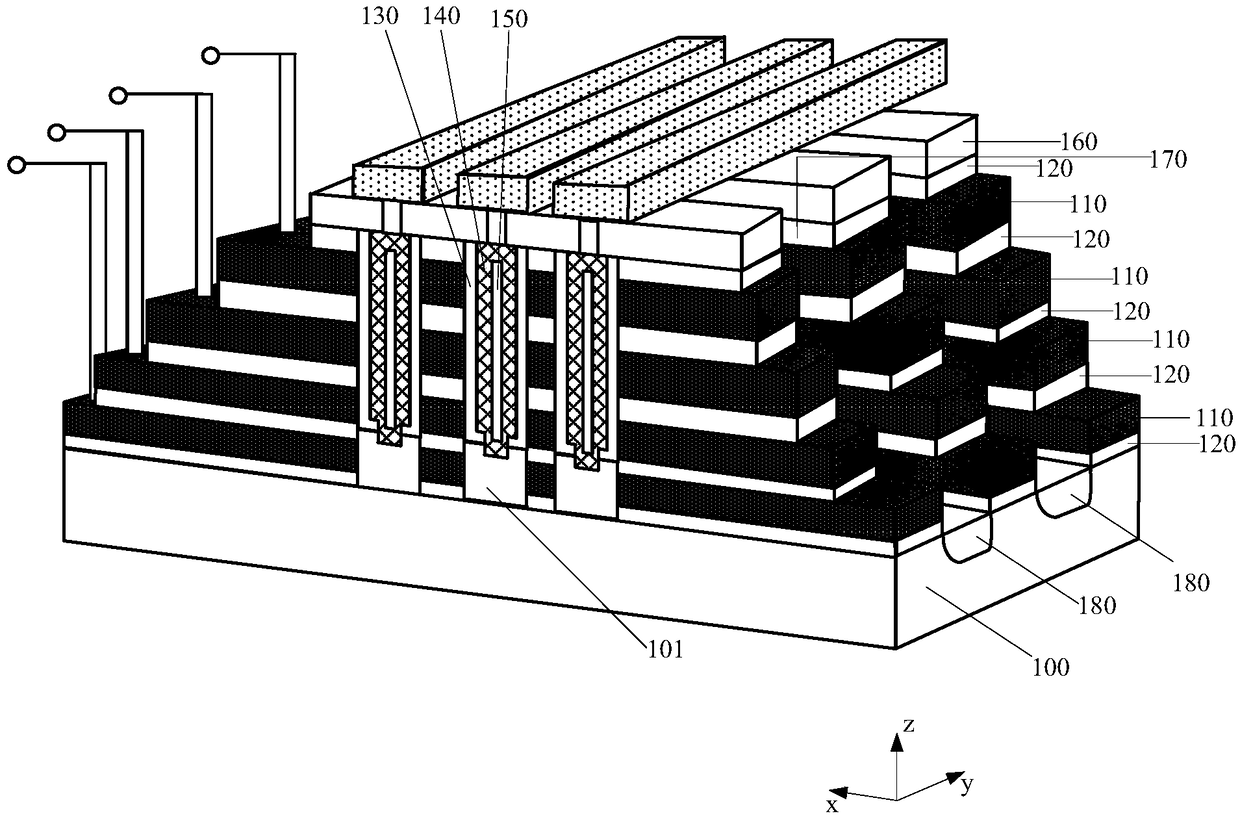
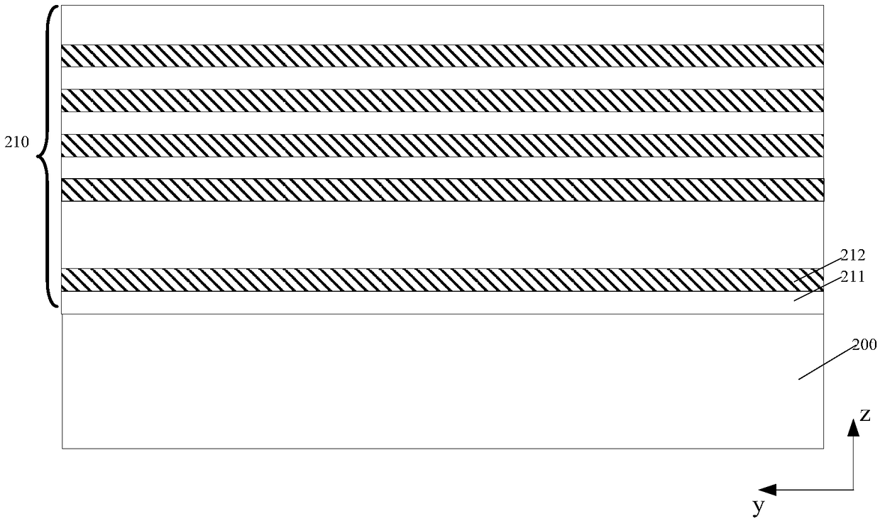
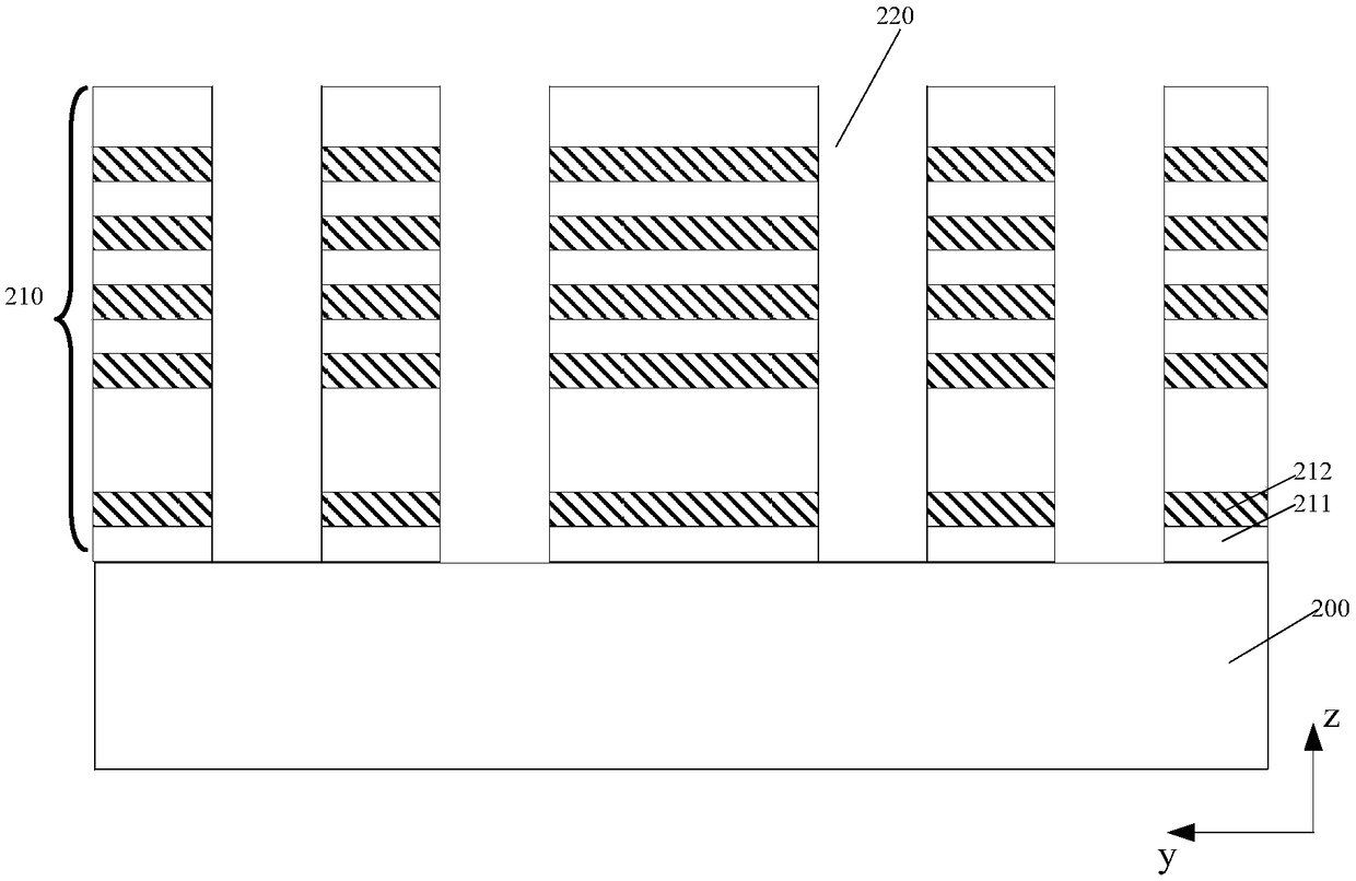
[0019] A kind of 3D-NAND flash memory, please refer to figure 1 , comprising: a semiconductor substrate 100; several layers of stacked conductive layers 110 on the semiconductor substrate 100; several layers of stacked insulating layers 120, the insulating layer 120 is located between the conductive layers 110 of adjacent layers, the bottom conductive layer 110 and between the semiconductor substrates 100, and on the conductive layer 110 of the top layer; a channel hole (not shown) penetrating through the conductive layer 110 and the insulating layer 120; the substrate extension region 101 at the bottom of the channel hole; The side wall of the hole and the intrinsic gate dielectric layer 130 on the surface of the substrate extension region 101, the channel layer 140, the channel layer 140 is located in the channel hole and on the surface of the in...


PUM

PropertyMeasurementUnit
Thicknessaaaaaaaaaa

Abstract

A 3D-NAND flash memory comprise a semiconductor substrate; A stack structure on the semiconductor substrate, the stack structure comprising a plurality of layers of insulating layers and a plurality of layers of conductive layers stacked in staggered layers; A channel structure penetrating the stack structure, The channel structure includes a high-K gate dielectric layer continuously distributed in a direction perpendicular to a semiconductor substrate, a channel sacrificial layer located between the high-K gate dielectric layer and the insulating layer, and a channel sacrificial layer separated by the conductive layer in a direction perpendicular to the semiconductor substrate. The performance of 3D-NAND flash memory is improved.

Description

technical field [0001] The invention relates to the field of semiconductor manufacturing, in particular to a 3D-NAND flash memory. Background technique [0002] Flash memory (Flash Memory) is also called flash memory. The main feature of flash memory is that it can keep stored information for a long time without power on, and has the advantages of high integration, fast access speed, easy erasing and rewriting, etc. , so it has become the mainstream memory of non-volatile memory. According to different structures, flash memory is divided into NOR Flash Memory and NAND Flash Memory. Compared with NOR Flash Memory, NAND Flash Memory can provide high cell density, high storage density, and faster writing and erasing speed. [0003] With the development of planar flash memory, the production process of semiconductors has made great progress. However, the current development of planar flash memory has encountered various challenges: physical limits, such as exposure technology...

Claims


Application Information

Patent Timeline
IPC IPC(8): H01L27/1157H01L27/11582H01L29/792
CPCH01L29/7926H10B43/35H10B43/27
Inventor 华文宇夏志良
Owner YANGTZE MEMORY TECH CO LTD
Features
  • R&D
  • Intellectual Property
  • Life Sciences
  • Materials
  • Tech Scout
  • Unparalleled Data Quality
  • Higher Quality Content
  • 60% Fewer Hallucinations
Learn More