

Epitaxial wafer for a diode
A technology of diodes and epitaxial wafers, applied in the field of epitaxial wafers, can solve problems such as easy loosening, damaged diodes, inconvenient fixing, etc., and achieve the effect of not being easy to loosen and eliminating static electricity
- Summary
- Abstract
- Description
- Claims
- Application Information
AI Technical Summary
Problems solved by technology
Method used
Image

Examples
Embodiment Construction
[0019] The following will clearly and completely describe the technical solutions in the embodiments of the present invention with reference to the accompanying drawings in the embodiments of the present invention. Obviously, the described embodiments are only some, not all, embodiments of the present invention. Based on the embodiments of the present invention, all other embodiments obtained by persons of ordinary skill in the art without making creative efforts belong to the protection scope of the present invention.
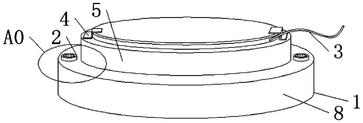
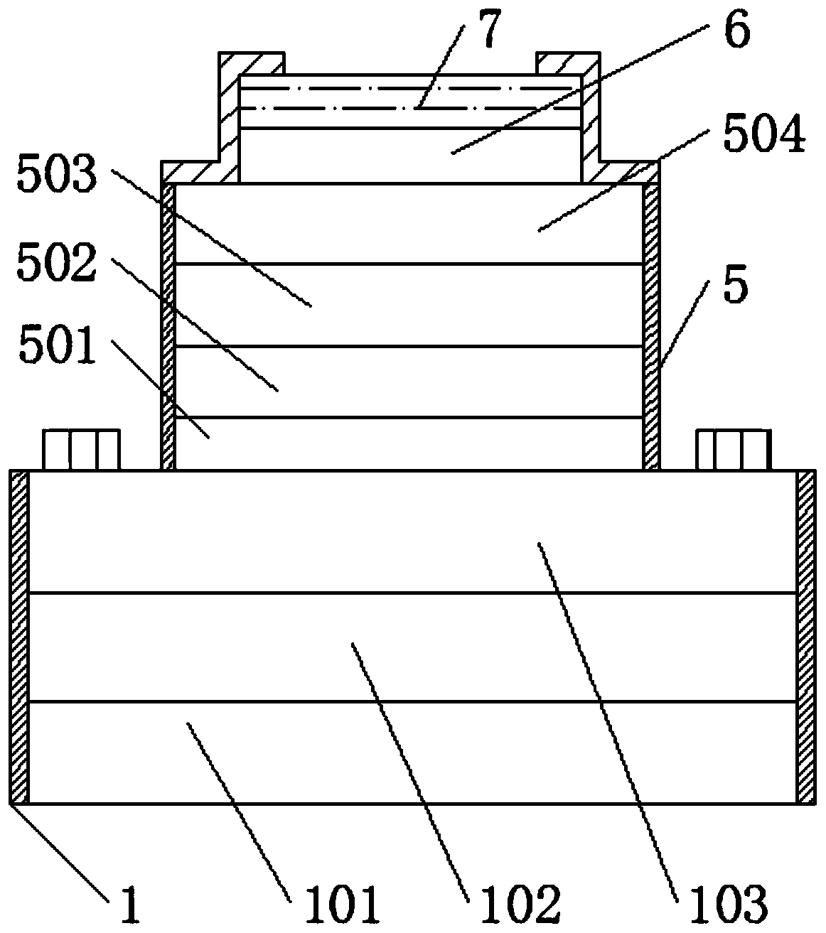
[0020] see Figure 1-3 , the present invention provides a technical solution: an epitaxial wafer for a diode, comprising an upper casing 5 and a lower casing 1, the upper casing 5 is arranged on the top of the lower casing 1; the inside of the lower casing 1 is provided with sapphire 101, non-doped gallium nitride 102 and n-type heavily doped gallium nitride 103, and the sapphire 101, non-doped gallium nitride 102 and n-type heavily doped gallium nitride 103 a...
PUM
 Abstract
Description
Claims
Application Information