Pixel-delimiting structure and preparation method thereof, and OLED device
A technology of pixel definition and pixel definition layer, which is applied in the manufacture of electric solid-state devices, semiconductor devices, semiconductor/solid-state devices, etc. The effect of avoiding color mixing and improving performance
- Summary
- Abstract
- Description
- Claims
- Application Information
AI Technical Summary
Problems solved by technology
Method used
Image

Examples
Embodiment 1
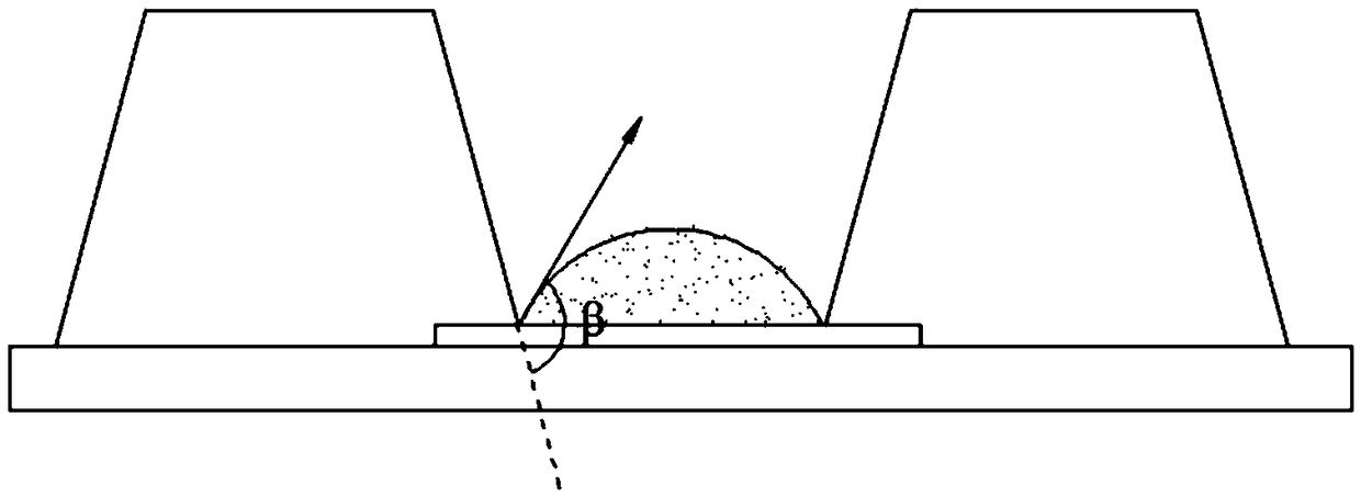
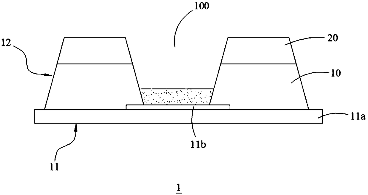
[0030] refer to figure 2 , in this embodiment, the pixel defining structure 1 includes a substrate 11 and a pixel defining film 12, the pixel defining film 12 includes two layers of pixel defining layers, and the two layers of pixel defining layers are sequentially stacked on the substrate 11 along the direction away from the substrate 11 On the top, that is, two layers of pixel defining layers are stacked sequentially from bottom to top on the substrate 11. In this embodiment, the pixel defining layer at the bottom of the pixel defining film 12 is called the first pixel defining layer 10, and the 12 The top pixel defining layer is called the second pixel defining layer 20, the first pixel defining layer 10 is hydrophilic, and the second pixel defining layer 20 is hydrophobic.
[0031] The substrate 11 includes a TFT array layer 11a and a transparent electrode layer 11b, the transparent electrode layer 11b is disposed on the TFT array layer 11a, and the transparent electrode ...
Embodiment 2
[0053] refer to Figure 5 The difference between this embodiment and Embodiment 1 is that the pixel defining film 12 includes N layers of pixel defining layers, and the N layers of pixel defining layers are sequentially stacked on the substrate 11 along the direction away from the substrate 11, that is, N layers of pixel The defining layers are sequentially stacked on the substrate 11 from bottom to top. In this embodiment, the N layers of pixel defining layers are referred to as the first pixel defining layer, the second pixel defining layer, . . . For the N-1th pixel defining layer and the Nth pixel defining layer, the first pixel defining layer is hydrophilic, and the Nth pixel defining layer is hydrophobic.
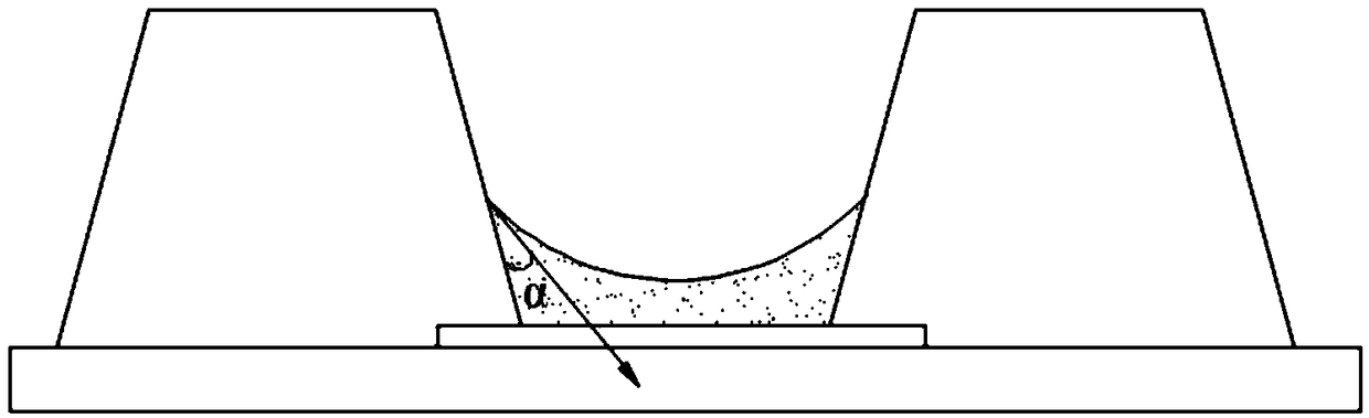
[0054] The hydrophilicity of the material used for the first pixel defining layer can make the contact angle between the first pixel defining layer and the ink of organic luminescent material be 0°-60°, wherein the contact angle of the first pixel defining layer and t...
PUM
| Property | Measurement | Unit |
|---|---|---|
| Thickness | aaaaa | aaaaa |
Abstract
Description
Claims
Application Information
 - R&D
- Intellectual Property
- Life Sciences
- Materials
- Tech Scout
- Unparalleled Data Quality
- Higher Quality Content
- 60% Fewer Hallucinations
Browse by: Latest US Patents, China's latest patents, Technical Efficacy Thesaurus, Application Domain, Technology Topic, Popular Technical Reports.
© 2025 PatSnap. All rights reserved.Legal|Privacy policy|Modern Slavery Act Transparency Statement|Sitemap|About US| Contact US: help@patsnap.com