Flexible OLED display panel

A display panel, flexible technology, applied in the direction of photovoltaic power generation, electrical components, circuits, etc., can solve the problems of different stress and deformation, affecting the bending and folding of the display panel, and achieve the effects of dispersing stress, increasing the area, and eliminating stress Effect

Active Publication Date: 2019-01-11
WUHAN CHINA STAR OPTOELECTRONICS SEMICON DISPLAY TECH CO LTD
View PDF10 Cites 23 Cited by
  • Summary
  • Abstract
  • Description
  • Claims
  • Application Information

AI Technical Summary

Problems solved by technology

[0004] The invention provides a flexible OLED display panel, which can increase the contact area between each film layer, disperse and eliminate the stress generated in the panel bending process, and solve the problem of the existing flexible display panel due to the multi-layer film layer structure. Superposition, resulting in different stress and deformation of each film layer, which in turn affects the bendability and foldability of the display panel

Method used


Image

  • Flexible OLED display panel
  • Flexible OLED display panel
  • Flexible OLED display panel

Examples


Embodiment 1

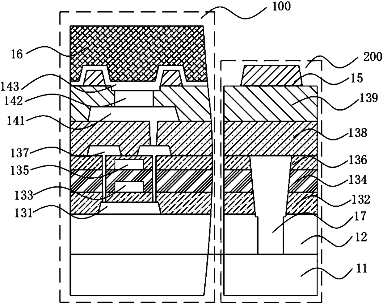
[0027] Such as figure 1 As shown, this embodiment provides a flexible OLED display panel, on which a display area 100 and a bending area 200 are defined, and the flexible OLED display panel includes: a flexible substrate 11; a buffer layer 12, forming On the flexible substrate 11 ; the thin film transistor layer is formed on the buffer layer 12 , the OLED light emitting layer 14 is formed on the thin film transistor layer; the encapsulation layer 16 is formed on the surface of the OLED light emitting layer 14 .

[0028] Such as image 3 As shown, the flexible substrate 11 includes: a first polyimide layer 111; a first barrier layer 112, disposed on the surface of the first polyimide layer 111; a second polyimide layer 113, disposed on the surface of the first barrier layer 112 ; the second barrier layer 114 is disposed on the surface of the second polyimide layer 113 .

[0029] The first polyimide layer 111 is fabricated on a glass substrate (not shown in the figure), and af...

Embodiment 2

[0053] In this embodiment, except that the structure of the thin film transistor layer in the bending region 200 is different from that of the first embodiment, other structures are the same as those described in the first embodiment.

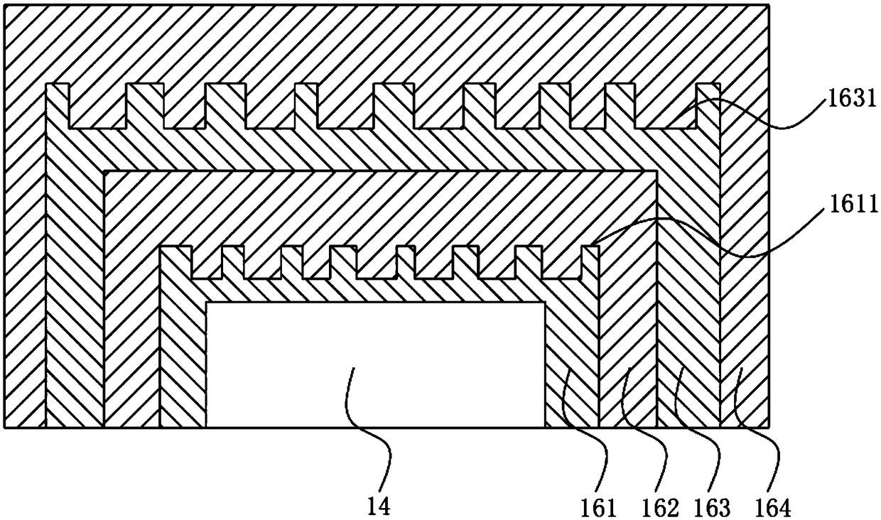
[0054] Such as Figure 4 As shown, in the bending region 200, the second gate insulating layer 134 includes a sixth top surface 1341 with a plurality of protrusions, the sixth top surface 1341 is away from the flexible substrate 11, the layer The lower surface of the inter-insulation layer 136 is in contact with the sixth top surface 1341 to form a concave-convex structure.

[0055] The planarization layer 138 includes a seventh top surface 1381 with a plurality of protrusions, the seventh top surface 1381 faces away from the flexible substrate 11 , the lower surface of the pixel definition layer 139 is in contact with the seventh top surface 1381 contacts to form a concave-convex structure.

[0056] In the bending region 200, by arranging mu...

Embodiment 3

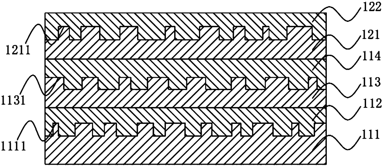
[0059] On the basis of embodiment two, in the film layer deposition process, the mode that adopts Mask (mask plate) to fully expose part film layer is completely removed, as Figure 5 shown.

[0060] In the bending area 200, the second polyimide layer 113 is provided with a plurality of first through holes 1132, and the second barrier layer 114 passes through the first through holes 1132 and the first barrier layer 112. For contact, in the photomask process, a full exposure method is used to form the first through hole 1132 .

[0061] The first buffer layer 121 is provided with a plurality of second through holes 1212 , and the second buffer layer 122 is in contact with the second barrier layer 114 through the second through holes 1212 .

[0062] The first gate insulating layer 132 is provided with a plurality of third through holes 1321 , and the second gate insulating layer 134 is in contact with the second buffer layer 122 through the third through holes 1321 .

[0063] T...


PUM


Abstract

A flexible OLED display panel is provided. The display panel comprises a flexible substrate, a buffer layer, a thin film transistor layer, an OLED light emitting layer and an encapsulation layer, wherein the encapsulation layer comprises a first inorganic layer, a first organic layer, a second inorganic layer and a second organic layer sequentially arranged on the OLED light emitting layer; Wherein the first inorganic layer includes a first top surface having at least two projections, the first top surface being opposite to the OLED light emitting layer. The second inorganic layer includes a second top surface having at least two projections, the second top surface facing away from the OLED light emitting layer. As that surface of each film layer is arrange in a concave-convex fit structure, the contact area between each film layer is effectively increased, and the stress generated in the bending proces of the panel is further dispersed and eliminated, thereby facilitating the bendingproperty of the OLED device to be realized.

Description

technical field [0001] The invention relates to the field of display technology, in particular to a flexible OLED display panel. Background technique [0002] At present, flexible OLED display panels are usually composed of multi-layer inorganic and organic structures layer by layer. Generally, flexible OLED display panels include flexible substrates, barrier layers, buffer layers, active layers, gate insulating layers, gate electrodes, and interlayer insulation. layer, source-drain layer, planarization layer, OLED light-emitting layer, pixel definition layer, support pad, packaging layer, etc., the multi-layer stacked film structure is limited by the deformation characteristics and stress of each layer of film material. With the development of display, currently flexible display screens are widely called curved screens because they can only present a fixed curved surface, and there is a certain distance from the goal of realizing flexible screens that can be bent and folded...

Claims


Application Information

Patent Timeline
Patent Type & Authority Applications(China)
IPC IPC(8): H01L51/52H01L27/32
CPCH10K59/127H10K50/84Y02E10/549H10K59/124H10K50/80H10K50/8445H10K2102/311H10K77/111
Inventor 张锋
Owner WUHAN CHINA STAR OPTOELECTRONICS SEMICON DISPLAY TECH CO LTD
Why Eureka
Try Eureka