
A low-power TO-277 package ultra-thin diode and a manufacturing method thereof

A TO-277, manufacturing method technology, applied in semiconductor/solid-state device manufacturing, electrical components, electric solid-state devices, etc., can solve problems affecting product life and reliability, thick body, large space occupation, etc., to achieve molding The process is simple, the power loss is reduced, and the production efficiency is improved.

Pending Publication Date: 2019-01-15
BINHAI ZHIRUN ELECTRONICS
View PDF0 Cites 2 Cited by
  • Summary
  • Abstract
  • Description
  • Claims
  • Application Information

AI Technical Summary

Problems solved by technology

At present, the thickness of conventional products in the market is relatively thick and takes up a lot of space, which has been unable to keep up with the changes in the market.
The main function of the diode is to convert the alternating current in the line into direct current. During the working process, it is easy to generate high temperature due to its own power consumption, which affects the service life and reliability of the product.

Method used


Image

  • A low-power TO-277 package ultra-thin diode and a manufacturing method thereof
  • A low-power TO-277 package ultra-thin diode and a manufacturing method thereof

Examples


Embodiment Construction

[0021] The implementation mode of the present invention is illustrated by specific specific examples below, and those who are familiar with this technology can easily understand other advantages and effects of the present invention from the content disclosed in this specification.

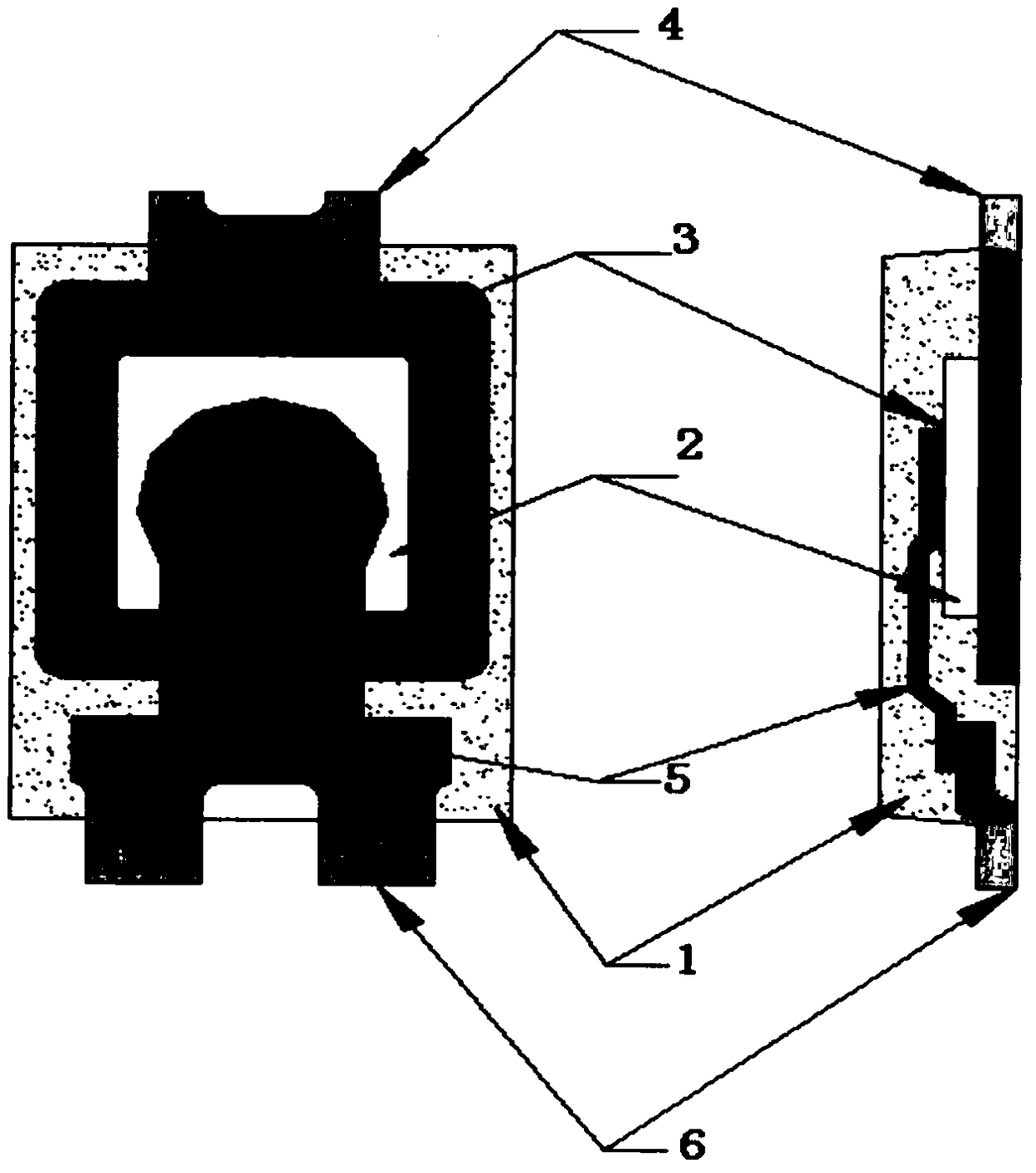
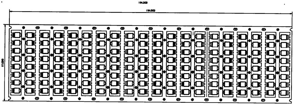
[0022] The invention provides a low-power consumption TO-277 package ultra-thin diode product, figure 1 It is a diagram of the low-power consumption TO-277 package ultra-thin diode product of the present invention, 01-plastic package, 02-chip, 03-solder, 04-material, 05-jumper, 06-tinning. figure 2 It is a diagram of a matrix material of the low-power consumption TO-277 packaged ultra-thin diode product of the present invention. The chip, solder, jumper wire and part of the material are packaged in the black plastic package, and the part of the material is extended to the black plastic package as a pin, and the surface of the pin is tinned to facilitate welding. The cross-section of the plastic p...


PUM


Abstract

The invention provides a low-power TO-277 package ultra-thin diode comprising a black glue plastic seal body, a chip, a material sheet, a jumper wire, solder and lead tin plate, wherein that chip, thesolder, the jumper wire and a part of the material sheet are encapsulated in the black glue plastic seal body, and the material sheet part extends to the black glue plastic seal body as a lead, and the surface of the lead is convenient to be soldered after tin plating; The cross section of the black glue plastic sealing body is isosceles trapezoid, the height of the black glue plastic sealing body is 1.1 mm, and the pins are linear and are in a straight line with the lower surface of the plastic sealing body. Compared with the existing packages, the overall package thickness can be reduced bymore than 40%; The product adopts low forward voltage chip, which can reduce power loss by 20% and meet the requirement of six-level energy efficiency. In the production process, the bending foot molding process is eliminated, and the lead pin can be cut directly, so that the stress generated by the bending foot can be removed, and the bad conditions such as the bending foot cannot be caused, andthe product quality is guaranteed; Matrix sheet design, simple molding process, improve production efficiency, reduce production costs.

Description

technical field [0001] The invention relates to a packaged ultra-thin diode, in particular to a low-power consumption TO-277 packaged ultra-thin diode and a manufacturing method thereof, belonging to the field of semiconductor electronic components. Background technique [0002] With the development of semiconductor technology in the direction of high density and high integration, electronic products have become smaller and thinner. With the development of electronic products, semiconductor devices are also developing in the direction of miniaturization and flattening. demand for different products. At present, the thickness of conventional products in the market is relatively thick and takes up a lot of space, which has been unable to keep up with the changes in the market. The main function of the diode is to convert the alternating current in the line into direct current. During the working process, it is easy to generate high temperature due to its own power consumption...

Claims


Application Information

Patent Timeline
Patent Type & Authority Applications(China)
IPC IPC(8): H01L23/495H01L23/31H01L21/48H01L21/60
CPCH01L24/85H01L21/4842H01L23/3121H01L23/49562H01L2224/85H01L2224/40245H01L2224/32245H01L2924/181H01L2924/00012
Inventor 薛敬伟王锡胜胡长文
Owner BINHAI ZHIRUN ELECTRONICS
Learn More