Supercharge Your Innovation With Domain-Expert AI Agents!

A method for manufacturing a semiconductor device

A manufacturing method, semiconductor technology, applied in semiconductor/solid-state device manufacturing, electric solid-state devices, resistors, etc., can solve problems such as long circuit delay time, small size, resistance and capacitance delay, etc.

Inactive Publication Date: 2019-01-15
SHANGHAI HUAHONG GRACE SEMICON MFG CORP
View PDF12 Cites 0 Cited by
  • Summary
  • Abstract
  • Description
  • Claims
  • Application Information

AI Technical Summary

Problems solved by technology

[0005] The object of the present invention is to provide a kind of manufacturing method of semiconductor device, to solve the problem that the size of semiconductor device is too small in the prior art, and resistance capacitance delay causes circuit delay time to be long

Method used


Image

  • A method for manufacturing a semiconductor device
  • A method for manufacturing a semiconductor device
  • A method for manufacturing a semiconductor device

Examples


Embodiment Construction

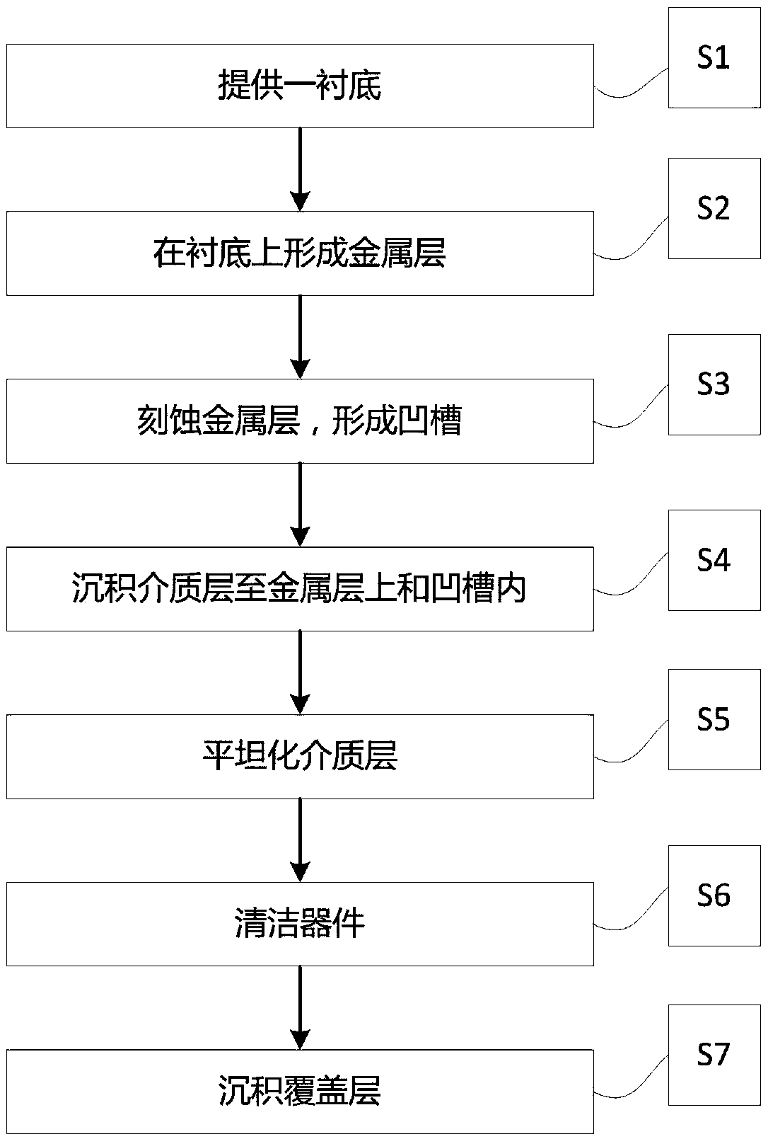
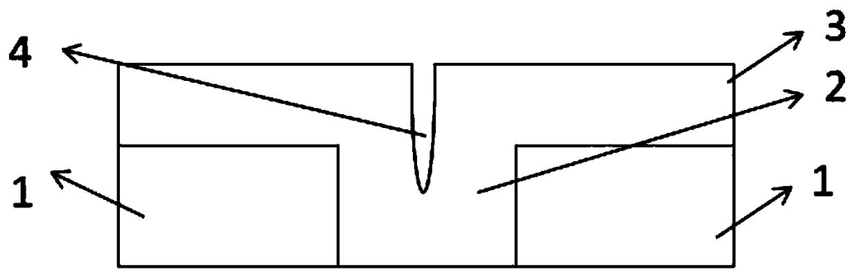
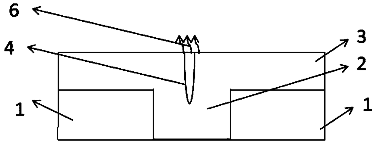
[0027] The specific implementation manner of the present invention will be described in more detail below with reference to schematic diagrams. Advantages and features of the present invention will be apparent from the following description and claims. It should be noted that the drawings are all in a very simplified form and use imprecise scales, and are only used to facilitate and clearly assist the purpose of illustrating the embodiments of the present invention.

[0028] In the following description, it will be understood that when a layer (or film), region, pattern or structure is referred to as being "on" a substrate, layer (or film), region and / or pattern, it can be directly on another layer or substrate, and / or intervening layers may also be present. Further, it will be understood that when a layer is referred to as being 'under' another layer, it can be directly under, and / or one or more intervening layers may also be present. In addition, designations regarding 'on...


PUM


Abstract

The invention relates to a method of manufacturing a semiconductor device, comprising the following steps: providing a substrate, wherein a metal layer is formed on the substrate, and a groove is provided in the metal layer; Depositing a dielectric layer onto the metal layer and in the groove, at the groove, forming a gap in the dielectric layer; Performing planarization processing on the dielectric layer; Cleaning the gap; And depositing a cover layer onto the dielectric layer and covering the gap. The invention adopts air gap process to reduce the influence of resistance and capacitance delay of devices with size smaller than 0.25 micron, and removes the grinding liquid and cleaning liquid flowing into the gap by cleaning the gap. After removal of the abrasive liquid and the cleaning liquid, the gap is free of liquid volatility in a subsequent deposition process, helping to compact the overlay deposition so that the gap is uniform and controllable. Uniform and controllable gaps improve capacitance consistency and hence resistance-capacitance delay.

Description

technical field [0001] The invention relates to a manufacturing method of a semiconductor device, in particular to a manufacturing method capable of improving a semiconductor device with an air cavity gap. Background technique [0002] At present, the main reasons for the time delay in the circuit are gate delay (Gate delay) and resistor capacitor delay (RCdelay). When the device size is smaller than 0.25um, the time delay (RC delay) caused by the parasitic elements of the interconnection line will exceed the gate delay (Gate delay) of the circuit, becoming the main bottleneck restricting the speed of the integrated circuit. [0003] In the prior art, in order to reduce the impact of RC delay, FSG and IMD air gap processes are usually used. For the air gap process, the height of the air gap will become higher with the increase of the Metal pitch. The higher air gap will be exposed after IMDCMP, and the grinding liquid and cleaning liquid will flow into it, affecting the IM...

Claims


Application Information

Patent Timeline
Patent Type & Authority Applications(China)
IPC IPC(8): H01L49/02H01L21/02H10N97/00
CPCH01L28/20H01L28/40H01L28/90H01L21/02065
Inventor 徐杰黄冲李志国周洋胡海天
Owner SHANGHAI HUAHONG GRACE SEMICON MFG CORP
Features
  • R&D
  • Intellectual Property
  • Life Sciences
  • Materials
  • Tech Scout
  • Unparalleled Data Quality
  • Higher Quality Content
  • 60% Fewer Hallucinations
Learn More