A microstrip vertical transition structure

A vertical transition, microstrip technology, applied in electrical components, connecting devices, circuits, etc., can solve the problems of narrow relative bandwidth, complex processing, parasitic effects, etc., achieve wide relative bandwidth, meet the requirements of height and transmission frequency band, reduce The effect of parasitic effects

Pending Publication Date: 2019-01-15
成都博芯联科科技有限公司
View PDF0 Cites 7 Cited by
  • Summary
  • Abstract
  • Description
  • Claims
  • Application Information

AI Technical Summary

Problems solved by technology

[0004] The purpose of the present invention is to provide a vertical transition structure for microstrip lines in view of the above-mentioned problems, so as to solve the problems of complex processing, weak adaptability, narrow relative bandwidth and serious parasitic effects at high frequencies. question

Method used


Image

  • A microstrip vertical transition structure
  • A microstrip vertical transition structure
  • A microstrip vertical transition structure

Examples


Embodiment 1

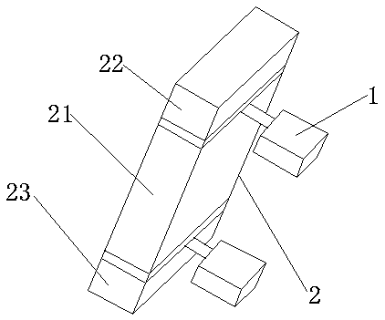
[0038] Such as figure 1 , the present invention is a microstrip vertical transition structure, including a microstrip section and a waveguide section 2; the microstrip section includes two microstrip boards 1, which are respectively inserted into the waveguide section 2 with a window in the center of the broadside.

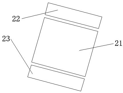
[0039] Such as figure 2 , the waveguide section 2 includes a waveguide cavity main body 21, and a waveguide cavity upper cover plate 22 and a waveguide cavity lower cover plate 23 respectively fastened with both ends of the waveguide cavity main body 21; A microstrip plate 2 is provided between the cover plate 22 and the lower cover plate 23 of the waveguide cavity.

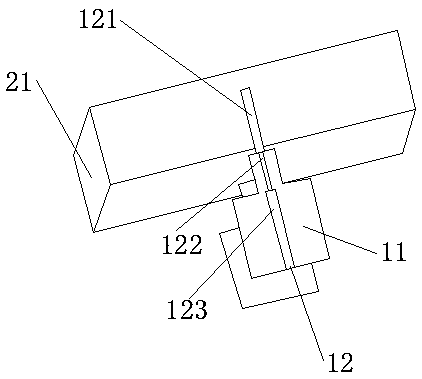
[0040] Such as image 3 , the microstrip board 1 includes a microstrip dielectric substrate 11, and a microstrip line 12 arranged on the top layer of the microstrip dielectric substrate 11; the microstrip dielectric substrate 11 is a four-layer PCB, and the top layer is etched as a microstrip line...

Embodiment 2

[0044] Such as Figure 4 , the present embodiment discloses a microstrip vertical transition structure, the waveguide cavity upper cover 22 and the waveguide cavity lower cover 23 respectively buckled at both ends of the waveguide cavity main body 21, and the waveguide cavity main body 21 and the waveguide cavity upper cover 22 respectively A microstrip dielectric substrate 11 is installed on the cross-section between the lower cover plate 23 of the waveguide cavity, and a microstrip dielectric substrate 11 is provided with a microstrip line 12, and the microstrip line 12 is respectively connected to an input joint and an output joint; The upper cover plate 22 of the waveguide cavity, the lower cover plate 23 of the waveguide cavity and the microstrip dielectric substrate 11 are fixed through the screw holes 222 .

[0045] Such as Figure 5 , the two ends of the waveguide cavity main body 21 are respectively provided with a microstrip dielectric substrate 11, the microstrip d...


PUM


Abstract

The invention discloses a microstrip vertical transition structure, which is characterized in that the microstrip vertical transition structure comprises a microstrip section and a waveguide section;The microstrip segment comprises two microstrip plates respectively inserted into the waveguide segments with the center window of the wide side; The waveguide section comprises a waveguide cavity main body, an upper cover plate of the waveguide cavity and a lower cover plate of the waveguide cavity respectively buckled with two ends of the waveguide cavity main body; The microstrip plate is respectively arranged between the waveguide cavity main body and the upper cover plate of the waveguide cavity, and between the waveguide cavity main body and the lower cover plate of the waveguide cavity.The invention adopts a microstrip-based method, which comprises the following steps of: Waveguide The form of microstrip has lower insertion loss, larger working bandwidth, compact structure, convenient processing and easy loading and unloading. And the height of the waveguide can be easily changed, which can be applied to more vertical transition requirements of the microstrip.

Description

technical field [0001] The invention relates to the field of microwave and millimeter wave multilayer circuits, in particular to a microstrip vertical transition structure. Background technique [0002] The microstrip vertical transition structure is an indispensable component in microwave and millimeter wave multilayer circuits. Various microwave and millimeter wave integrated circuits are widely used in modern wireless systems and radar systems. As the requirement for miniaturization becomes higher and higher, microwave and millimeter wave multilayer circuits are more and more widely used. [0003] Conventional microstrip line-to-microstrip line transition methods include: realizing the transition between upper and lower microstrip lines based on metal vias; realizing the transition between upper and lower layers of microstrip lines based on slot coupling; vertical transition of microstrip lines based on cavity coupling; microstrip line transition based on glass insulator...

Claims


Application Information

Patent Timeline
Patent Type & Authority Applications(China)
IPC IPC(8): H01P5/02
CPCH01P5/028
Inventor 张鹏举
Owner 成都博芯联科科技有限公司
Why Eureka
Try Eureka