Broadband slot-coupled multilayer microstrip antenna based on substrate-integrated waveguide feeding

A technology of waveguide feeding and substrate integration, which is applied in the direction of electrical short antennas, antennas, resonant antennas, etc., can solve the problems of insufficient stability of gain within the bandwidth and deterioration of antenna bandwidth gain, so as to save processing costs, widen antenna bandwidth, feed The effect of simple electrical structure

Inactive Publication Date: 2019-01-15
XIDIAN UNIV
View PDF2 Cites 11 Cited by
  • Summary
  • Abstract
  • Description
  • Claims
  • Application Information

AI Technical Summary

Problems solved by technology

Although these methods can broaden the antenna bandwidth, they may lead to deterioration of the gain within the antenna bandwidth and cause some problems for feeding
[0004] In the paper "Wide-Bandwidth 60-GHz Aperture-Coupled Microstrip Patch Antennas (MPAs) Fed by Substrate Integrated Waveguide (SIW)" published by Wael M. Abdel-Wahab, a substrate-integrated waveguide-fed broadband slot-coupled patch is proposed The antenna increases the bandwidth of the antenna by using the substrate integrated waveguide feed and slot coupling, but the relative bandwidth of the antenna is only 24.1%, and the gain within the bandwidth is not stable enough

Method used


Image

  • Broadband slot-coupled multilayer microstrip antenna based on substrate-integrated waveguide feeding
  • Broadband slot-coupled multilayer microstrip antenna based on substrate-integrated waveguide feeding
  • Broadband slot-coupled multilayer microstrip antenna based on substrate-integrated waveguide feeding

Examples


Embodiment Construction

[0018] Below in conjunction with accompanying drawing and specific embodiment, the present invention is described in further detail:

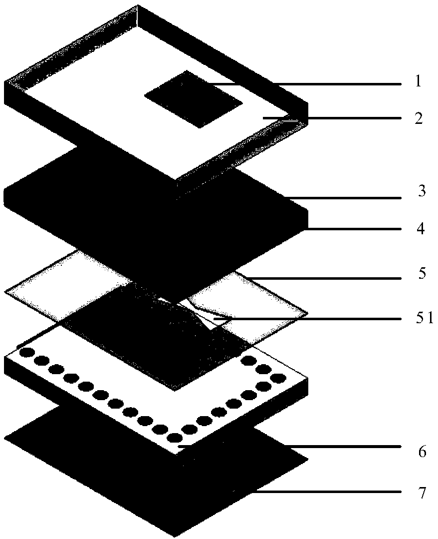
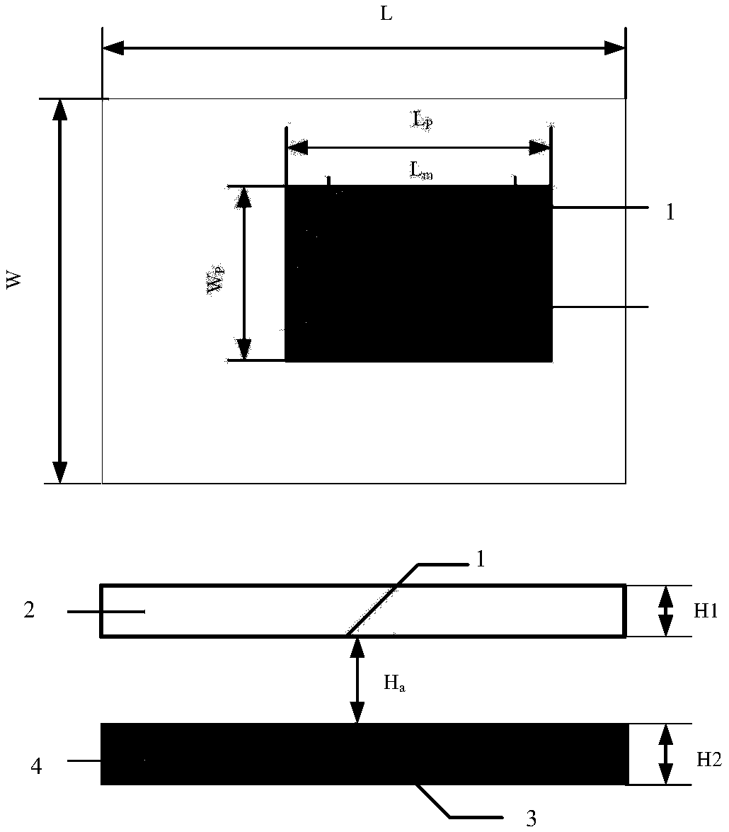
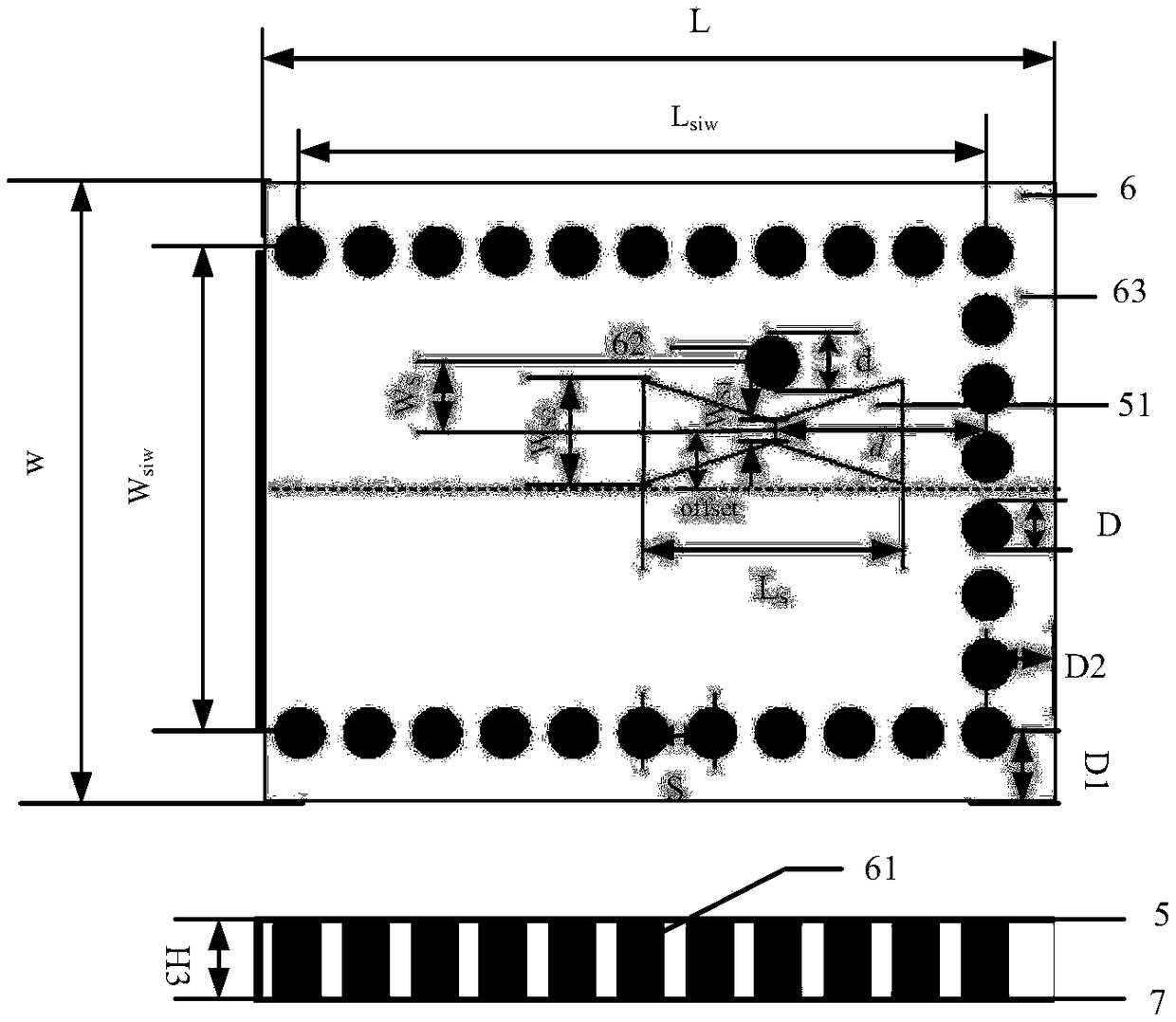
[0019] refer to figure 1 , this example includes a parasitic patch 1 , a first dielectric substrate 2 , a main radiation patch 3 , a second dielectric substrate 4 , an upper floor 5 , a feed structure 6 and a lower floor 7 . The parasitic patch 1 is located on the lower surface of the first dielectric substrate 2, the main radiation patch 3 is located on the upper surface of the second dielectric substrate 4, the upper floor 5 is located on the upper surface of the feeding structure 6, and the lower floor 7 is located on the upper surface of the feeding structure 5. On the lower surface, longitudinal slots 51 are etched on the upper floor 5 for coupling energy from the feed structure 6; an air layer is provided between the parasitic patch 1 and the main radiation patch 3 to widen the bandwidth of the antenna.

[0020] refer to figure 2 , the...


PUM


Abstract

The invention discloses a broadband slot coupling multi-layer microstrip antenna based on substrate integrated waveguide feeding, which mainly solves the problems of narrow band width and poor gain stability of the existing microstrip antenna. The antenna comprises a parasitic patch (1), a first dielectric substrate (2), a main radiation patch (3), a second dielectric substrate (4), an upper floor(5), a feeding structure (6) and a lower floor (7). The parasitic patch (1) is located on the lower surface of the first dielectric substrate (2), the main radiation patch (3) is located on the uppersurface of the second dielectric substrate (4), the upper floor (5) is located on the upper surface of the feeding structure (6), and the lower floor (7) is located on the lower surface of the feeding structure (6); A longitudinal gap (51) is etch on that upper floor (5) for coupling energy from the fee structure (6); An air layer is arranged between the parasitic patch (1) and the main radiationpatch (3) for widening the antenna bandwidth. The invention improves working bandwidth and gain stability, and can be applied to 5G communication and radar system.

Description

technical field [0001] The invention belongs to the technical field of antennas, and further relates to a broadband multilayer microstrip antenna, which can be used in 5G communication and radar systems. Background technique [0002] The substrate-integrated waveguide adopts printed circuit board PCB technology or low-temperature co-fired ceramic LTCC technology, etc., and forms two rows of parallel metallized through holes closely arranged on the dielectric substrate. Due to the small distance between the through holes, the electromagnetic wave can be limited to a certain level. Propagating forward within the range, a planar waveguide structure similar to a dielectric-filled waveguide can be formed. It has the advantages of small size, light weight, convenient PCB processing, low processing cost, and easy integration with microwave and millimeter wave integrated circuits, and has been applied in the field of antennas. [0003] Due to the high quality factor of the traditio...

Claims


Application Information

Patent Timeline
Patent Type & Authority Applications(China)
IPC IPC(8): H01Q9/04H01Q1/38H01Q1/48H01Q1/50
CPCH01Q1/38H01Q1/48H01Q1/50H01Q9/0457
Inventor 李龙李美灵易浩席瑞赵琦
Owner XIDIAN UNIV
Why Eureka
Try Eureka