A kind of laminated plate structure and pressing method of pcb pressing based on cushioning material

A cushioning material and board stacking technology, which is applied in multi-layer circuit manufacturing, printed circuit, electrical components, etc., can solve the problems of difficult control of the thickness accuracy of the board, hollow board, and inability to fully meet the requirements of temperature and pressure buffering, etc.

Active Publication Date: 2020-10-30
ANHUI SUN CREATE ELECTRONICS
View PDF4 Cites 0 Cited by
  • Summary
  • Abstract
  • Description
  • Claims
  • Application Information

AI Technical Summary

Problems solved by technology

[0003] The traditional PCB lamination method is to use kraft paper and silica gel pads as cushioning materials, when the thickness of the inner core board is not greater than 0.245mm and not less than 0.1mm, or the total thickness of the laminated plates after lamination is less than 1.0mm , and when the alignment accuracy of the sheets to be pressed is high, the traditional PCB lamination method is difficult to control the thickness accuracy of the sheets after pressing due to the uneven temperature and pressure of the sheets to be pressed. , The possibility of white spots on the laminated boards increases, and the quality problems of voids and layers may also appear inside the laminated boards
Therefore, the buffer materials used in traditional PCB lamination can no longer fully meet the requirements for temperature and pressure buffering in the PCB lamination process

Method used


Image

  • A kind of laminated plate structure and pressing method of pcb pressing based on cushioning material
  • A kind of laminated plate structure and pressing method of pcb pressing based on cushioning material

Examples


Embodiment 1

[0044] Embodiment 1, taking the lamination of a microwave twelve-layer board as an example.

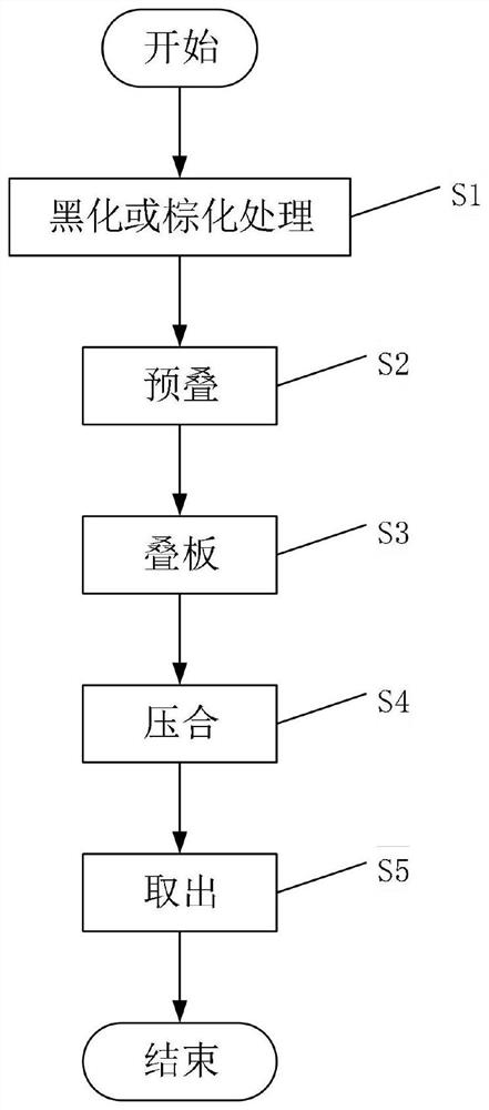
[0045] Depend on figure 2 Shown, a kind of pressing method of PCB pressing based on cushioning material, comprises the following steps:

[0046] S1, blackening or browning treatment is performed on the inner layer core board after the graphics are completed, and drying treatment is performed on the inner layer core board after the blackening or browning treatment; the blackening or browning treatment is to strengthen the inner layer The bonding force between the core board and the PP sheet.

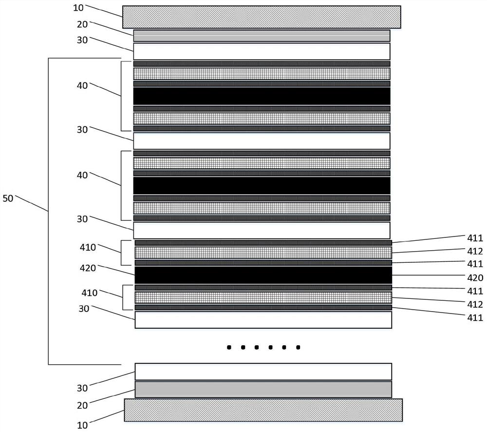
[0047] S2, pre-stacking, the pre-stacking is to stack and fix the inner layer core board and PP sheet together according to the lamination diagram required by the production, and the inner layer core board and PP sheet after stacking and fixing are the said to-be-pressed Sheet 420;

[0048] The superimposed and fixed process is a pin-positioning lamination process pin-lam or a pinless positio...

Embodiment 2

[0060] Embodiment 2, taking the lamination of microwave four-layer board as an example.

[0061] A kind of pressing method based on the PCB pressing of cushioning material, comprises the following steps:

[0062] S1, blackening or browning treatment is performed on the inner layer core board after the graphics are completed, and drying treatment is performed on the inner layer core board after the blackening or browning treatment; the blackening or browning treatment is to strengthen the inner layer The bonding force between the core board and the PP sheet.

[0063] S2, pre-stacking, the pre-stacking is to stack and fix the inner layer core board and PP sheet together according to the lamination diagram required by the production, and the inner layer core board and PP sheet after stacking and fixing are the said to-be-pressed Sheet 420;

[0064] The superimposed and fixed process is a pin-positioning lamination process pin-lam or a pinless positioning lamination process mass...


PUM

PropertyMeasurementUnit
thicknessaaaaaaaaaa
thicknessaaaaaaaaaa
thicknessaaaaaaaaaa

Abstract

The invention discloses a PCB laminating structure and method based on a buffer material, wherein the intermediate layer is a mirror steel plate and a laminated unit; The mirror steel plate is symmetrically distributed on the upper and lower sides of the lamination unit, a plurality of substrate units are arranged in the lamination unit, and mirror steel plates are arranged between adjacent substrate units. The substrate unit comprises: a plate to be pressed, a buffer layer symmetrically distributed on the upper and lower sides of the plate to be pressed; The buffer layer comprises a release film and a buffer material, and the release film is symmetrically distributed on the upper and lower sides of the buffer material; The buffer material is a prepreg. The FR The prepreg is used as cushioning material, which improves the uniformity of temperature and pressure in pressing process, is beneficial to the thickness control of plate, and avoids the appearance of white spots after pressing and the phenomenon of delamination, skateboard and deviation of layer inside the plate after pressing.

Description

technical field [0001] The invention relates to the technical field of lamination of printed multilayer circuit boards, in particular to a lamination structure and lamination method of PCB lamination based on cushioning materials. Background technique [0002] With the rapid development of the electronics industry, the requirements for printed circuit boards are getting higher and higher, the number of layers of printed circuit boards is increasing, the hole density of the circuit board is increasing and the hole diameter is small, and the number of holes on a circuit board is as high as There are thousands of them, and the hole diameters range from 0.05 to 2.0mm. With the development of thinner PCBs and more precise circuits, the requirements for PCB substrates are getting thinner and thinner, and the reliability requirements of PCB substrates are also getting higher and higher. [0003] The traditional PCB lamination method is to use kraft paper and silica gel pads as cus...

Claims


Application Information

Patent Timeline
Patent Type & Authority Patents(China)
IPC IPC(8): H05K3/46
CPCH05K3/4611
Inventor 戴银海陈彦青朱忠翰沈岳峰管美章崔良端牛顺义范晓春邓健彭腾金俊
Owner ANHUI SUN CREATE ELECTRONICS
Why Eureka
Try Eureka