A microdevice mass transfer device and method based on differential speed matching of transfer axes

A technology for transferring devices and micro-devices, which is applied in the manufacturing of semiconductor devices, electric solid-state devices, and semiconductor/solid-state devices, and can solve problems such as low efficiency and inability to meet the requirements of mass transfer of micro-devices.

Active Publication Date: 2019-01-18
HUAZHONG UNIV OF SCI & TECH
View PDF4 Cites 3 Cited by
  • Summary
  • Abstract
  • Description
  • Claims
  • Application Information

AI Technical Summary

Problems solved by technology

In this process, Micro-LEDs need to be transferred in batches. The existing Micro-LED transfer technology generally uses a robot to pick up micro-devices and then transfer

Method used


Image

  • A microdevice mass transfer device and method based on differential speed matching of transfer axes
  • A microdevice mass transfer device and method based on differential speed matching of transfer axes
  • A microdevice mass transfer device and method based on differential speed matching of transfer axes

Examples


Embodiment Construction

[0054] In order to make the object, technical solution and advantages of the present invention clearer, the present invention will be further described in detail below in conjunction with the accompanying drawings and embodiments. It should be understood that the specific embodiments described here are only used to explain the present invention, not to limit the present invention. In addition, the technical features involved in the various embodiments of the present invention described below can be combined with each other as long as they do not constitute a conflict with each other.

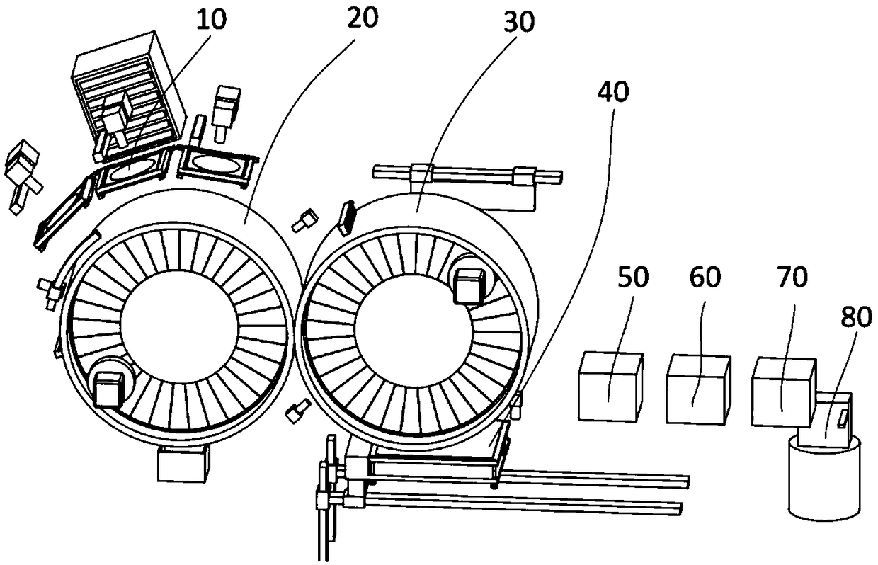
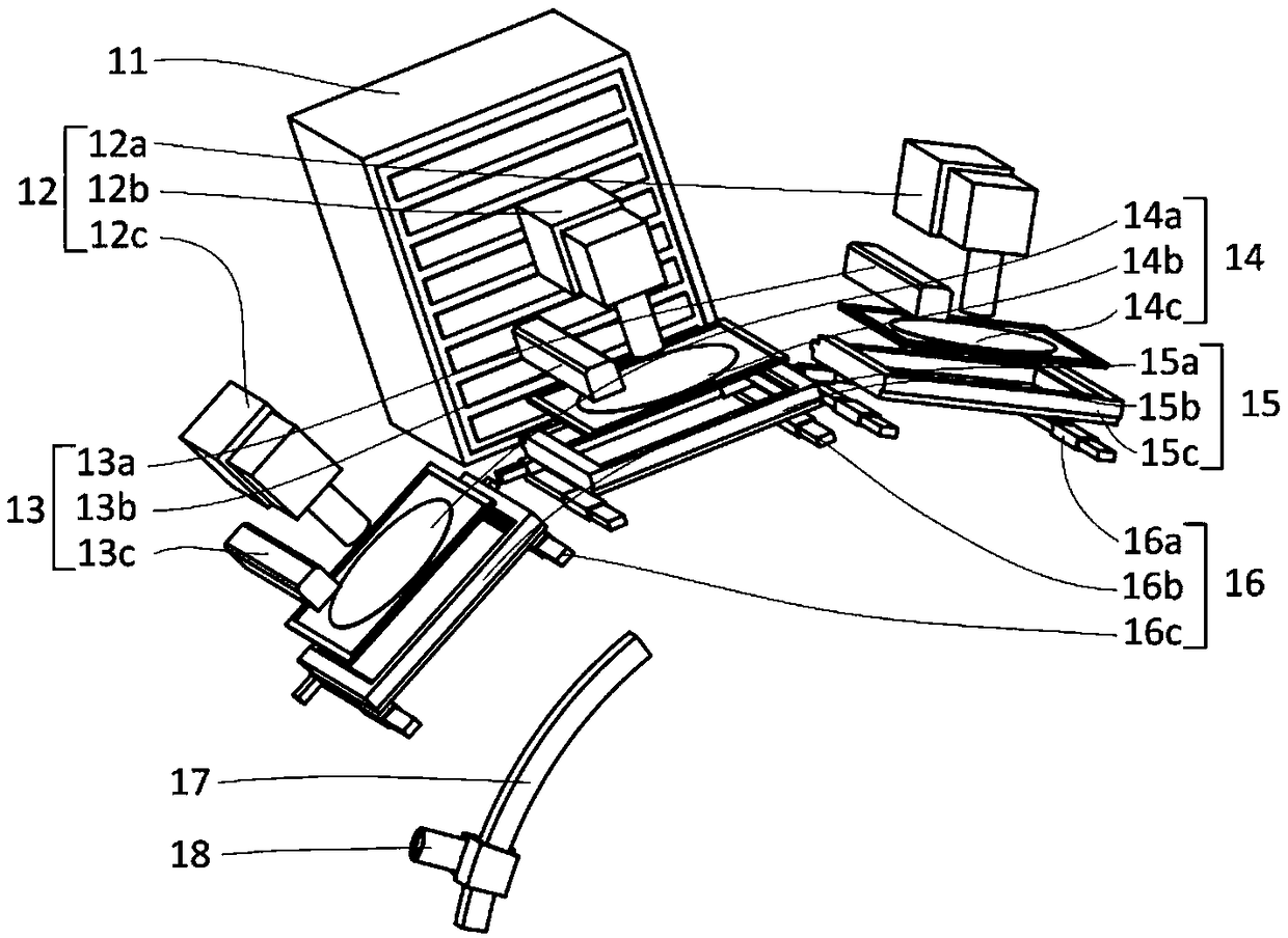
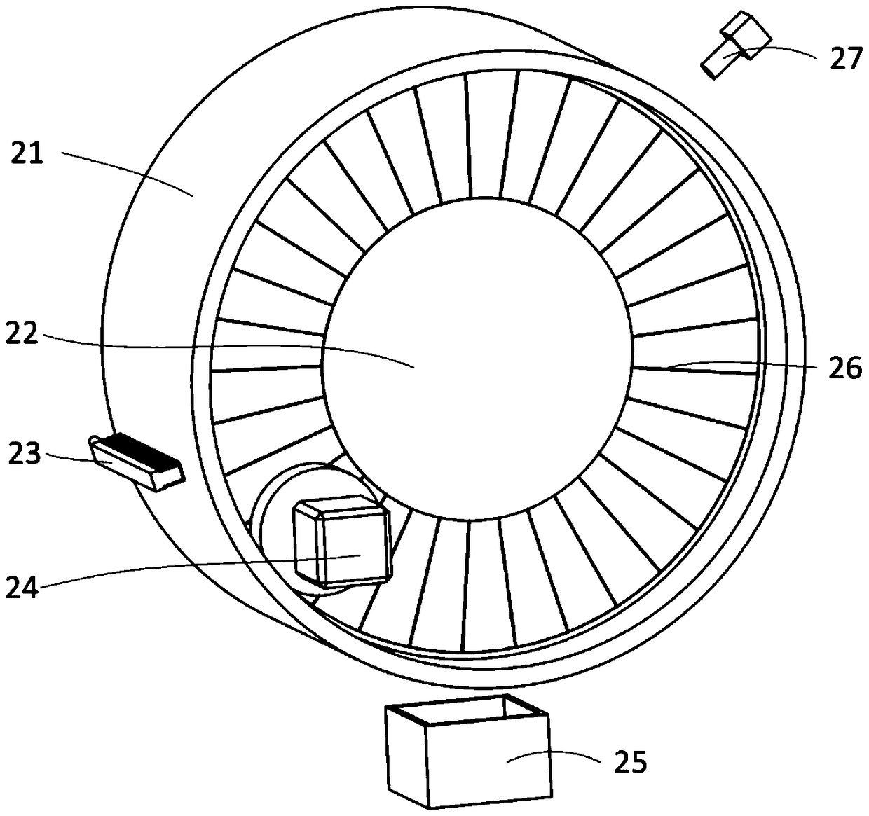
[0055] Such as figure 1 As shown, the embodiment of the present invention provides a micro-device mass transfer device based on transfer shaft differential speed matching, which includes a micro-device peeling transfer module 10, a primary transfer shaft module 20, a secondary transfer shaft module 30, The substrate carrying module 40, the micro-device filling module 50, the curing module 60, t...


PUM


Abstract

The invention belongs to the technical field of semiconductors, and particularly discloses a micro device mass transfer device and method based on differential speed matching of transfer axes, which comprises a microdevice stripping transfer module, a primary transfer shaft module, a secondary transfer shaft module, a substrate bearing module, a microdevice filling module, a curing module, a packaging module and a substrate handling module, wherein the microdevice stripping transfer module is used for stripping and transferring the microdevice to the primary transfer shaft module; The primarytransfer shaft module is used for picking up the microdevices and adjusting the spacing of the microdevices. The secondary transfer shaft module is used for picking up the microdevices on the primarytransfer shaft module and adjusting the spacing of the microdevices; The substrate carrying module is used for picking up the micro devices on the secondary transfer shaft module and sending them intothe micro device filling module, the curing module, the encapsulation module and the substrate handling module to realize filling, curing, encapsulation and loading and unloading. The invention realizes the massive transfer of the micro device by using the differential speed matching of the transfer shaft, which has the advantages of high production efficiency and low production cost.

Description

technical field [0001] The invention belongs to the technical field of semiconductors, and more specifically relates to a micro device mass transfer device and method based on differential speed matching of transfer shafts. Background technique [0002] Micro-LEDs refer to LEDs with extremely small sizes, whose size can reach several microns, and thousands or hundreds of Micro-LEDs can be prepared in the millimeter range to form a Micro-LED array. Due to the advantages of localized light emission, uniform current expansion, high saturation current density, high output optical power density, and high photoelectric modulation bandwidth, Micro-LEDs have shown good application prospects in the fields of display, maskless lithography, and visible light communication. . Due to its self-illuminating properties, it is also easier to realize low-power and high-brightness displays. [0003] The preparation of Micro-LED display screens first needs to prepare thin-film, miniaturized, ...

Claims


Application Information

Patent Timeline
IPC IPC(8): H01L21/677H01L27/15
CPCH01L21/67706H01L21/67721H01L27/156
Inventor 陈建魁尹周平金一威
Owner HUAZHONG UNIV OF SCI & TECH
Why Eureka
Try Eureka