
Silicon carbide schottky diode for optimizing heat distribution and method of manufacturing the same

A technology of Schottky diode and manufacturing method, which is applied in semiconductor/solid-state device manufacturing, electrical components, circuits, etc., can solve the problems of high temperature, lower rated current of devices, uneven current distribution, etc., to achieve uniform heat distribution, suppression of The effect of current concentration and optimized heat distribution

Pending Publication Date: 2019-01-18
WUXI NCE POWER
View PDF0 Cites 8 Cited by
  • Summary
  • Abstract
  • Description
  • Claims
  • Application Information

AI Technical Summary

Problems solved by technology

For silicon carbide diodes, the rated current refers to the current that can work continuously for a long time. When the existing silicon carbide diodes conduct current, the current density in the center of the chip is higher than that at the edge of the chip, which causes the temperature in the center of the chip to be higher than that at the edge of the chip. This phenomenon of uneven current distribution will seriously reduce the rated current of the device

Method used


Image

  • Silicon carbide schottky diode for optimizing heat distribution and method of manufacturing the same
  • Silicon carbide schottky diode for optimizing heat distribution and method of manufacturing the same
  • Silicon carbide schottky diode for optimizing heat distribution and method of manufacturing the same

Examples


Embodiment approach

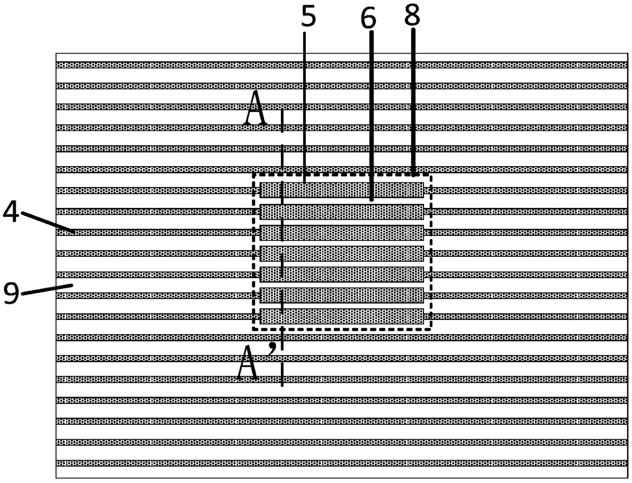
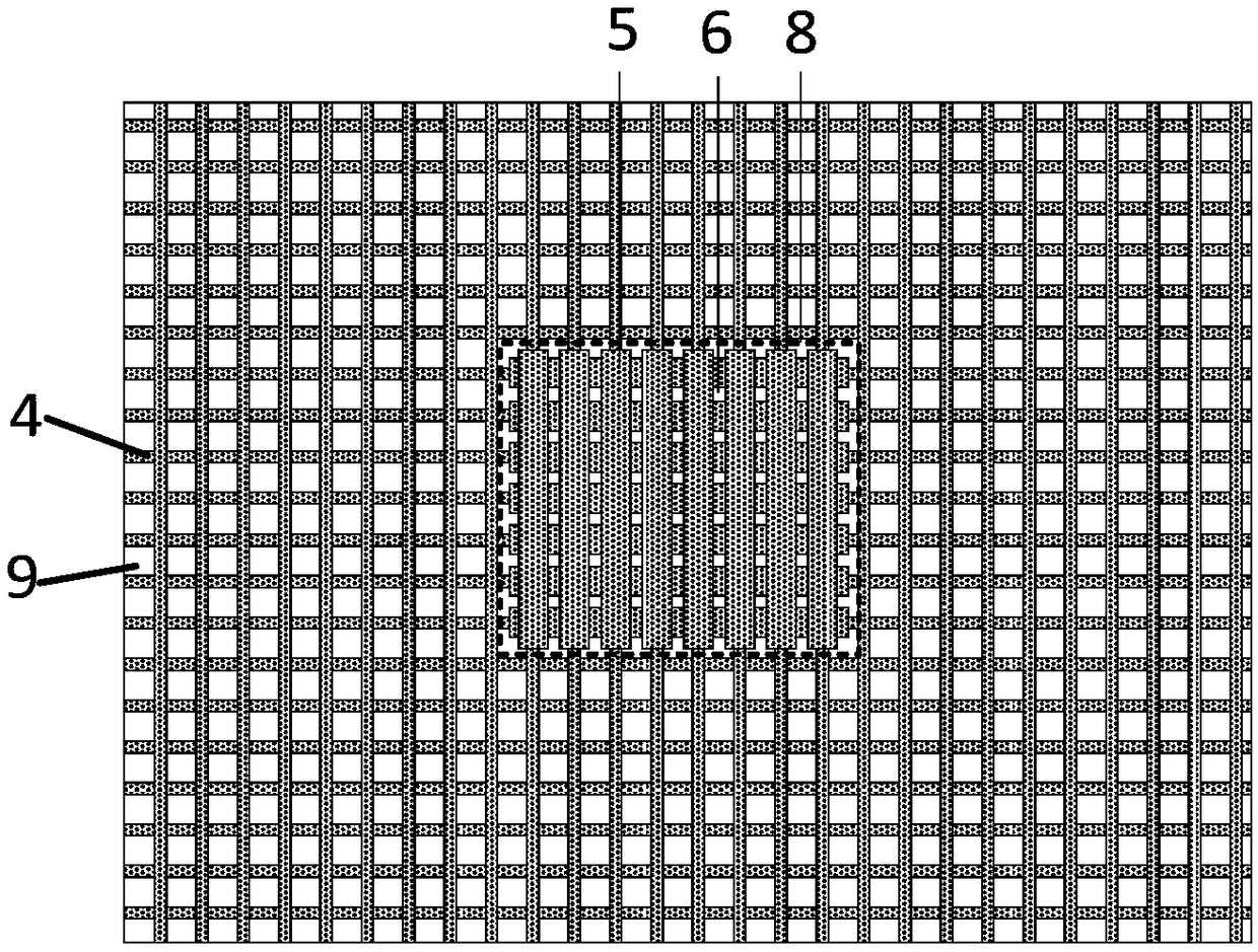
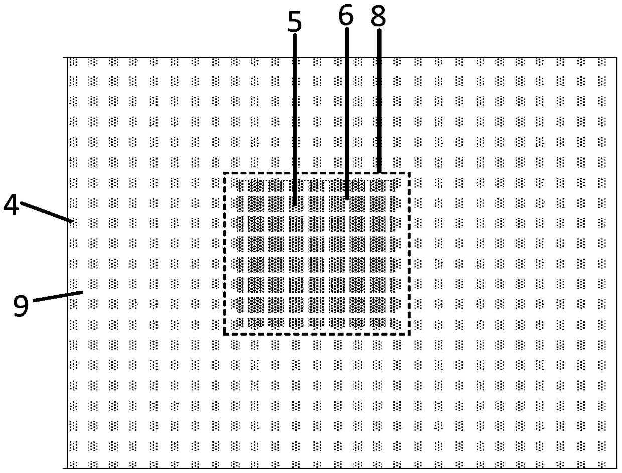
[0041] The first embodiment is as figure 1 As shown, it specifically includes the following steps:

[0042] S310: Form a current suppression region 8 in the middle of the upper surface of the N-type epitaxial layer 3, and inject P-type impurities into the upper surface of the N-type epitaxial layer 3 at the position of the current suppression region 8, thereby forming a strip-shaped second P Type well regions 5 and strip-shaped second N-type well regions 6, the second P-type well regions 5 and the second N-type well regions 6 are alternately distributed in the N-type epitaxial layer 3;

[0043] S320: Implanting P-type impurities on the upper surface of the N-type epitaxial layer 3 around the current suppression region 8, thereby forming a strip-shaped first P-type well region 4 and a strip-shaped first N-type well region 9, the first The P-type well regions 4 and the first N-type well regions 9 are distributed alternately at intervals around the current suppression region 8, ...


PUM


Abstract

The invention relates to the technical field of semiconductors, and discloses a silicon carbide Schottky diode for optimizing heat distribution and a method for manufacturing the same. A cathode motor, an N-type silicon carbide substrate, an N-type epitaxial lay and an anode electrode are sequentially arranged from bottom to top; the upper surface of the N-type epitaxial layer is formed with a current suppressing region in the middle, A plurality of second P-type well regions are spaced apart in the current suppression region, and a plurality of first P-type well regions are spaced apart on anupper surface of an N-type epitaxial layer around the current suppression region, wherein the area proportion of the second P-type well regions in the current suppression region is larger than that of the first P-type well regions on the chip-removed current suppression region. By reducing the current density in the center of the chip, the invention obviously reduces the temperature in the centerof the chip, so that the temperature distribution of the chip is uniform and the rated current of the device is improved.

Description

technical field [0001] The invention relates to the technical field of semiconductors, in particular to a silicon carbide Schottky diode with optimized heat distribution and a manufacturing method thereof. Background technique [0002] Power devices and their modules provide an effective way to realize the conversion of various forms of electric energy, and have been widely used in national defense construction, transportation, industrial production, medical and health and other fields. Since the first power device application in the 1950s, each generation of power devices has enabled more efficient conversion and use of energy. [0003] Traditional power devices and modules are dominated by silicon-based power devices, mainly thyristors, power PIN devices, power bipolar junction devices, power MOSFETs, and insulated gate field-effect transistors, which have been widely used in the full power range. Application, with its long history, very mature design technology and proce...

Claims


Application Information

Patent Timeline
Patent Type & Authority Applications(China)
IPC IPC(8): H01L29/872H01L29/06H01L21/04
CPCH01L29/0603H01L29/6606H01L29/872
Inventor 朱袁正周锦程杨卓
Owner WUXI NCE POWER
Learn More