A multicast broadcast communication-aware optical network-on-chip architecture and communication method

An optical on-chip network, multicast broadcasting technology, applied in the field of communication, can solve the problems of high power consumption, communication method delay and power consumption, poor scalability, etc., to reduce power consumption, reduce the number of photoelectric conversion and configuration time Overhead, the effect of reducing the number of uses

Active Publication Date: 2021-06-08
XIDIAN UNIV
View PDF4 Cites 0 Cited by
  • Summary
  • Abstract
  • Description
  • Claims
  • Application Information

AI Technical Summary

Problems solved by technology

[0009] The purpose of the present invention is to overcome the deficiencies in the above-mentioned prior art, and propose a multicast broadcast communication-aware optical on-chip network architecture, which is used to solve the problems of high power consumption and poor scalability of the optical on-chip network architecture in the prior art. Poor technical problems, as well as technical problems with large delays and power consumption in communication methods

Method used


Image

  • A multicast broadcast communication-aware optical network-on-chip architecture and communication method
  • A multicast broadcast communication-aware optical network-on-chip architecture and communication method
  • A multicast broadcast communication-aware optical network-on-chip architecture and communication method

Examples


Embodiment 2

[0077] The structure of Embodiment 2 is the same as that of Example 1, and the following parameters are adjusted:

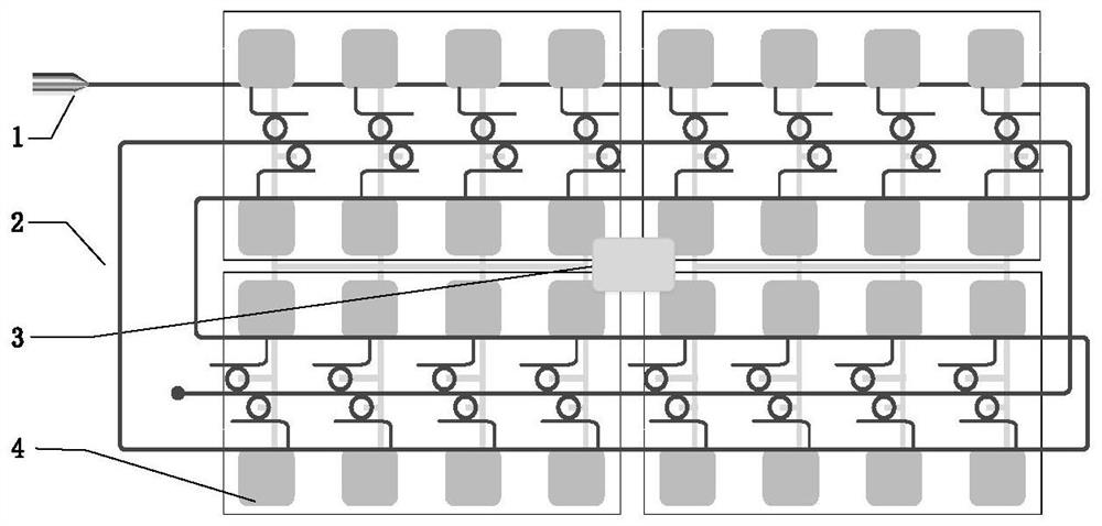
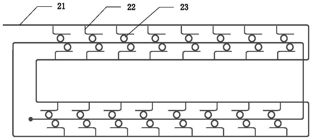
[0078] The 8 processor module 4 forms 1 cluster of 1 × 1 array arrangement, and a cluster contains an array of 2 x 4 processor module 4.

Embodiment 3

[0079] The structure of Embodiment 3 is the same as that of Example 1, and the following parameters are adjusted:

[0080] The 256 processor module 4 forms 32 clusters arranged in a 16 × 16 array, and includes an array of 2 x 4 processor module 4 in each cluster.

[0081] Refer Figure 7 , A communication method of a network architecture on a multicast broadcast communication perceived, including the following steps:

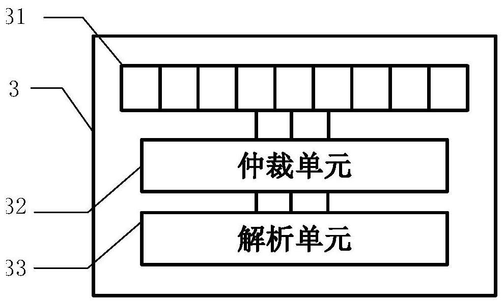
[0082] Step 1) Send a communication request to the global control unit as the processor module of the source node:

[0083] Step 1A) The processor checks for a private first-level cache sends request;

[0084] Step 1B) Private first-level cache determines whether or not the processor core request is stored. If this is transmitted to the processor core, the communication is ended, otherwise, the request is sent to the shared secondary cache, and perform step 1C);

[0085] Step 1c) Sharing the secondary cache determines whether or not to store the requested data, if th...


PUM


Abstract

The present invention proposes a multicast broadcast communication-aware optical network architecture on chip and a communication method, which are used to solve the technical problems of high power consumption and poor scalability of the optical network architecture existing in the prior art, and the communication method The existing technical problems of delay and power consumption are large. In the optical network architecture, the processor modules are divided into clusters arranged in arrays. Each cluster contains an array composed of 2×4 processor modules. Each The processor module is coupled and connected to a first active microring resonator through a coupling port, and the clusters arranged in the array are connected through a serpentine optical waveguide structure and expanded in units of clusters. At the same time, the first active microring resonator and The coupling distance distribution between optical waveguides is set by the power split system principle. In the communication method, the global control unit processes the communication request of the processor module, and sends the obtained control information to the multi-wavelength laser source and the first active microring resonator for network communication configuration.

Description

Technical field [0001] The present invention belongs to the field of communication technology, and in particular, the present invention relates to a network architecture and communication method on a multicast broadcast communication perceived, which can be used to calculate multicast broadcast communication between the processor modules in the system chip. Background technique [0002] As the number of processor cores integrated on a single chip have exponentially growth, the high performance communication between the processor core is the key to the performance improvement of the system. On-board network-based network-based networks can effectively improve processor nuclear communication performance, becoming a preferred solution for nuclear computing systems on the film. With the continuous expansion of the on-chip network and the development of high performance computing applications, the current interconnect-based online network faces the bandwidth, delay, and power consumpt...

Claims


Application Information

Patent Timeline
Patent Type & Authority Patents(China)
IPC IPC(8): H04Q11/00
CPCH04Q11/0005H04Q11/0067H04Q11/0071H04Q2011/0007H04Q2011/0047H04Q2011/0079
Inventor 顾华玺赵龙杨银堂王琨王康
Owner XIDIAN UNIV
Why Eureka
Try Eureka