Quantum dot light-emitting layer, quantum dot light-emitting device and preparation method
A quantum dot luminescence, quantum dot technology, applied in semiconductor/solid state device manufacturing, semiconductor device, electric solid device and other directions, can solve the problems of quantum dot quenching, quantum dot agglomeration, etc., to improve luminescence performance, improve color purity, The effect of increasing the width of the emission spectrum
- Summary
- Abstract
- Description
- Claims
- Application Information
AI Technical Summary
Problems solved by technology
Method used
Image
Examples
preparation example Construction
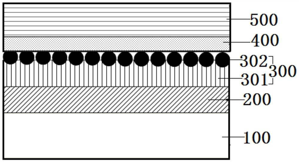
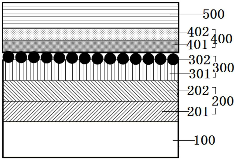
[0044] As an example, the preparation method of the quantum dot light-emitting layer includes: providing a metal-organic framework raw material solution, coating the metal-organic framework raw material solution on a substrate or a functional layer, and drying to form a metal-organic framework layer.
[0045] The quantum dot raw material solution is provided, the quantum dot raw material solution is coated on the metal organic framework layer, dried, and the quantum dots are embedded in the pores of the metal organic framework layer to obtain the quantum dot light-emitting layer.
[0046] According to the specific structure of the quantum dot light-emitting device to be prepared, the quantum dot light-emitting layer can be selectively formed on the substrate or the functional layer, wherein the functional layer can be a hole transport layer or an electron transport layer.
[0047] It can be understood that both the metal-organic framework raw material solution and the quantum dot...
example 3
[0058] As Example 3, the quantum dot light-emitting device includes: a transparent conductive electrode, a quantum dot light-emitting layer, and a metal electrode stacked sequentially from bottom to top. At this time, the quantum dot light-emitting device is an electroluminescent device without a transport layer structure, which is not shown in the figure.
[0059] Among them, for the hole transport layer and the electron transport layer mentioned in Example 1 and Example 2, the hole transport layer can be a separate hole transport layer, or it can be a stacked hole injection sublayer and a hole transport layer. layer. Likewise, the electron transport layer may be a single electron transport layer, or may be a laminated electron injection sublayer and electron transport sublayer.
[0060] The materials of the above functional layers are common in the art, and the following are examples respectively:
[0061] The electron injection sublayer can be LiF, NaF, LiQ, Li, and the t...
PUM
| Property | Measurement | Unit |
|---|---|---|
| diameter | aaaaa | aaaaa |
| thickness | aaaaa | aaaaa |
| thickness | aaaaa | aaaaa |
Abstract
Description
Claims
Application Information

