Reaction chamber and semiconductor processing device

A reaction chamber and reaction chamber technology, applied in discharge tubes, electrical components, circuits, etc., can solve problems such as poor symmetry of deep hole sidewall coverage, lack of directionality of metal atoms, unsatisfactory film deposition effects, etc.

Pending Publication Date: 2019-02-01
BEIJING NAURA MICROELECTRONICS EQUIP CO LTD
View PDF0 Cites 8 Cited by
  • Summary
  • Abstract
  • Description
  • Claims
  • Application Information

AI Technical Summary

Problems solved by technology

[0003] During the process, since the magnetron 5 passes through the middle region of the target more times than the center region and the edge region of the target, the distribution of the film deposited on the workpiece to be processed is uneven
On the other hand, due to the lack of good directionality of the metal atoms released from the target, for the deep holes of the workpiece to be processed, especially the deep holes in the edge area, only part of the direction of the metal atoms can be deposited on the side wall of the deep hole, which affects the The coverage of the sidewall of the deep hole, and part of the sidewall of the deep hole is more difficult to be deposited by metal ions, resulting in poor symmetry of the coverage of the sidewall of the deep hole
Especially the sidewall position close to the bottom of the deep hole, due to the high aspect ratio of this position, the film deposition effect at this position is not satisfactory

Method used


Image

  • Reaction chamber and semiconductor processing device
  • Reaction chamber and semiconductor processing device
  • Reaction chamber and semiconductor processing device

Examples


Embodiment Construction

[0040] In order to make the purpose, technical solutions and advantages of the present disclosure clearer, the present disclosure will be further described in detail below in conjunction with specific embodiments and with reference to the accompanying drawings.

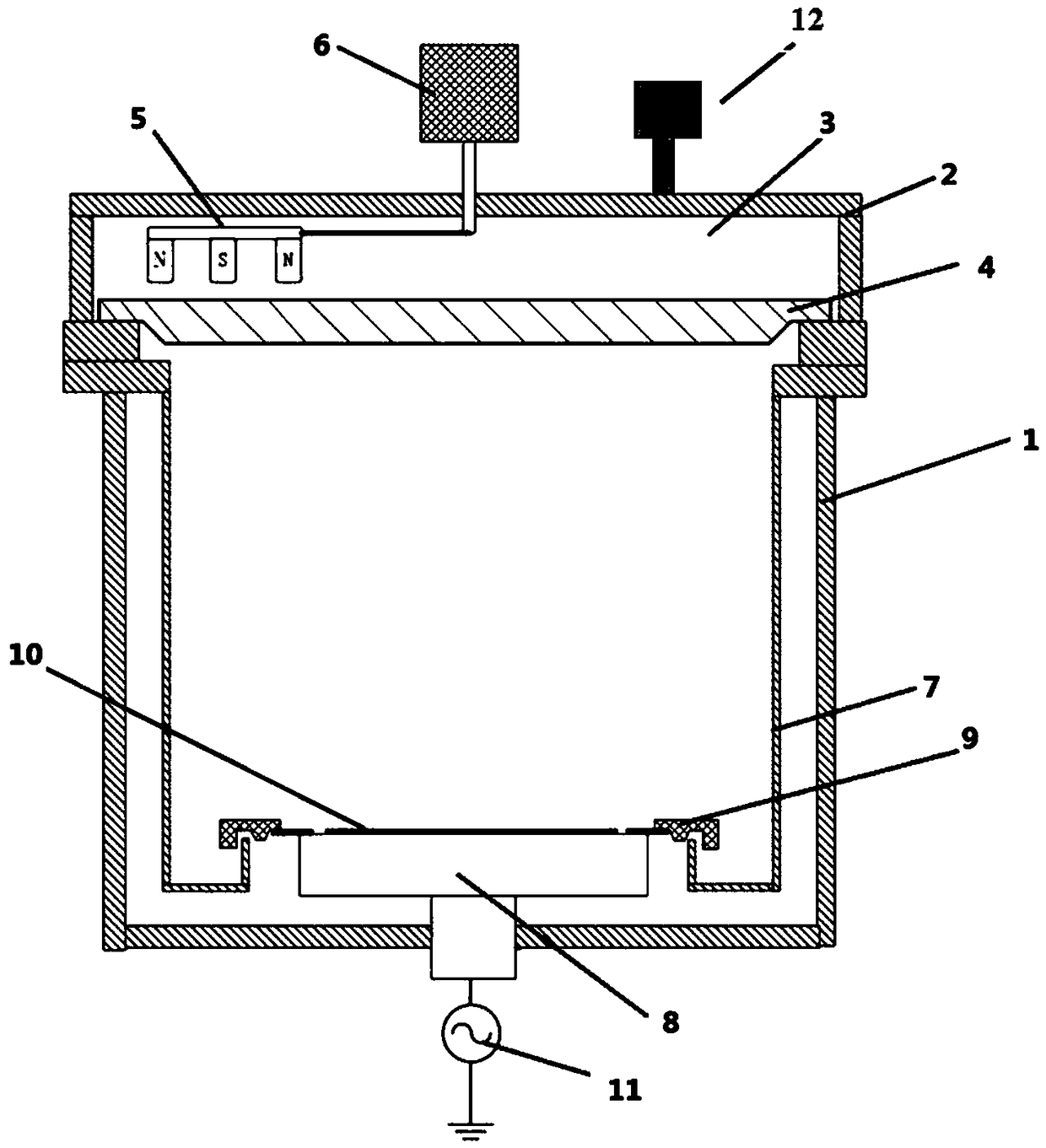
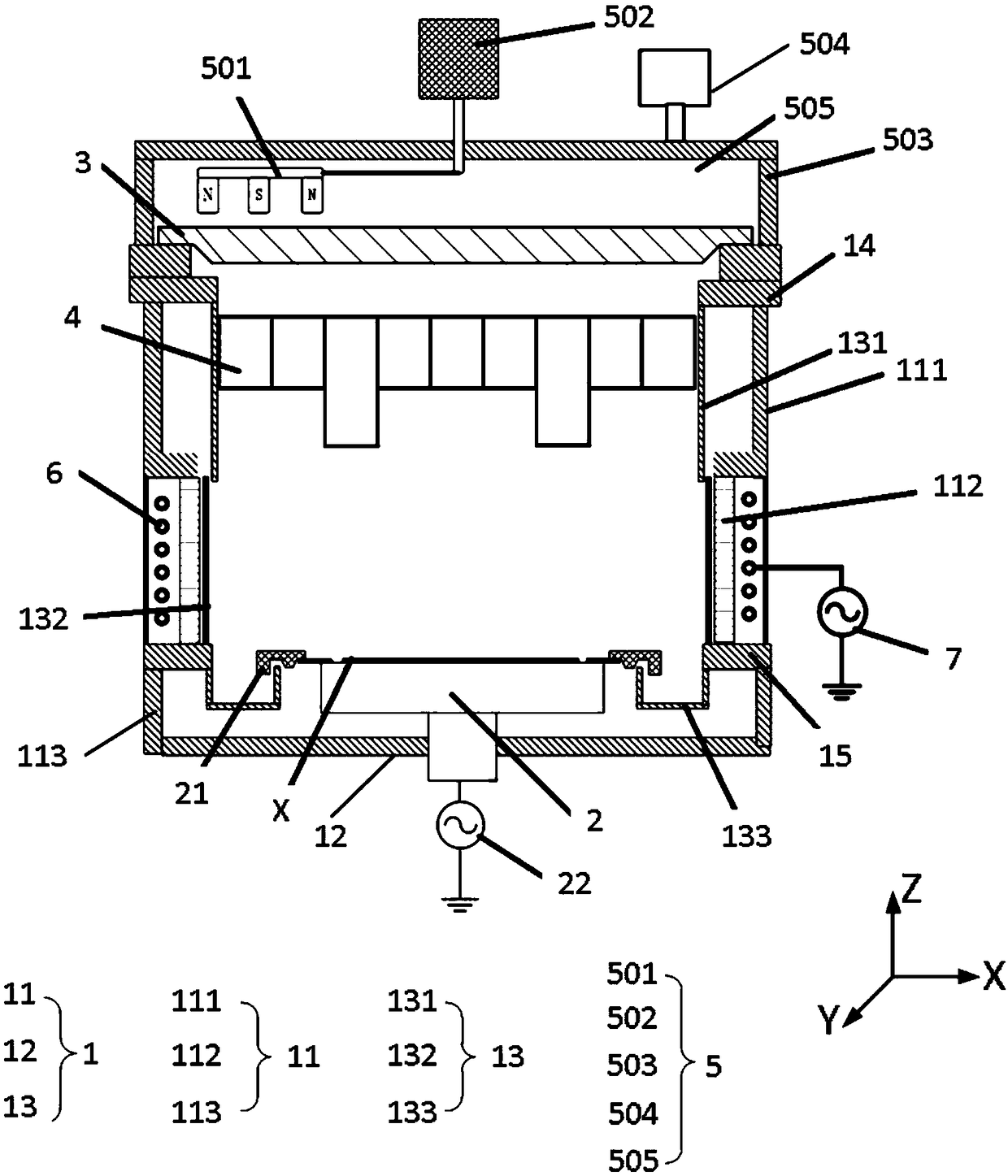
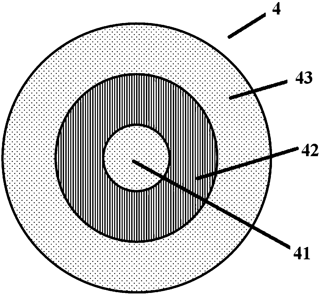
[0041] An embodiment of the present disclosure provides a reaction chamber, such as figure 2 As shown, the reaction chamber includes: a chamber body 1 , a base 2 , a target 3 and a collimator 4 .

[0042] The base 2 is arranged in the lower space of the reaction chamber, specifically, it may be arranged at the bottom of the chamber body 1 , and is used to carry the workpiece X to be processed, and the RF power is applied by the RF power supply 22 . A pressure ring 21 is also provided around the workpiece X to be processed, for fixing the position of the workpiece X to be processed on the base 2 .

[0043] The target material 3 is arranged in the upper space of the reaction chamber, specifically, it may be arranged o...


PUM


Abstract

The invention provides a reaction chamber, and the reaction chamber comprises a substrate which is used for bearing a to-be-processed workpiece; a target material which is disposed in the upper spaceof the reaction chamber; and a collimator which is disposed in a space below the target material and above a to-be-processed workpiece, so as to improve the symmetry of the coverage rate of the bottomof a deep hole of the to-be-processed workpiece and the coverage rate of the side wall of the deep hole. The invention also provides a semiconductor processing device.

Description

technical field [0001] The present disclosure relates to the technical field of semiconductor manufacturing, in particular to a reaction chamber and semiconductor processing equipment. Background technique [0002] Magnetron sputtering physical vapor deposition is a widely used method in the field of semiconductor manufacturing. Existing magnetron sputtering physical vapor deposition equipment such as figure 1 As shown, there is a grounded reaction chamber 1 . The base 8 is located in the reaction chamber 1 and carries the workpiece 10 to be processed. The snap ring 9 is placed around the workpiece 10 to be processed. The target 4 seals the reaction chamber 1 . The support assembly 2 and the target material 4 form a sealed cavity, which is filled with deionized water 3 . During the process, the driving device 6 drives the magnetron 5 to scan the surface of the target 4 , and the magnetron 5 passes back and forth between the central area and the edge area of ​​the target...

Claims


Application Information

Patent Timeline
Patent Type & Authority Applications(China)
IPC IPC(8): H01J37/34
CPCH01J37/3447H01J37/3408
Inventor 侯珏
Owner BEIJING NAURA MICROELECTRONICS EQUIP CO LTD
Why Eureka
Try Eureka