Method of monolithic integration of hyperspectral image sensor

a monolithic integration and image sensor technology, applied in the field of hyperspectral imaging, can solve the problems of slow analysis speed, increased non-uniformity, and high cost, and achieve excellent deposition uniformity, reduce device failure rate, and increase yield

Active Publication Date: 2017-10-12
INST OF MICROELECTRONICS CHINESE ACAD OF SCI
View PDF5 Cites 4 Cited by
  • Summary
  • Abstract
  • Description
  • Claims
  • Application Information

AI Technical Summary

Benefits of technology

[0017]As the atomic layer deposition process has a feature of excellent deposition uniformity, hence in the present disclosure, the N step structures formed on the bottom reflecting layer by using the area selective atomic layer deposition (ASALD) process have the same height within wafer. Thereby, with the method for monolithic integration of a hyperspectral image sensor according to the present disclosure, the problem of height non-uniformity of step structures within wafer is greatly minimized. Heights of the formed step structures are determined by conditions of the area selective atomic layer deposition process, for example, the number of deposition cycles. And, film deposition non-uniformity (<1.5%) of the ALD process is much smaller than that of the photolithography-etching process (2.7%) in practical (for example, ALD-Al2O3 films). Hence, with the method for monolithic integration of a hyperspectral image sensor according to the present disclosure, the problem of non-uniformity accumulation due to the etching process in conventional technology is greatly minimized. Thereby, it is beneficial to reduce device failure rate so to increase the yield.
[0018]In addition, the ALD process can be used to generate various types of film materials which are not necessarily to be etched easily. Hence, compared with the photolithography-etching process, the method for monolithic integration of a hyperspectral image sensor according to the present disclosure can be applied more widely in the aspect of material selection of a cavity layer.

Problems solved by technology

A previous hyperspectral imaging system is based on laboratory setups, therefore it slows in analysis speed, high in cost and not compact at all.
Practically, it is reported that etching depths have within wafer non-uniformity of at least about 2.7% during each etching process, which means that the more etching steps are performed, the greater the non-uniformity.
As a transparent cavity layer composed of multiple step structures requires multiple etching steps, thus, accumulation of the non-uniformity increases as the etching steps increases.
Therefore, the device may be failed due to being out of the specifications.
In addition, it is difficult to apply plasma etching or wet etching to etch some specific materials, for example, hafnium(IV) oxide (HfO2).
Since the boiling points of the halides of the lanthanide transition metals (including Hf) are high (higher than 300 degrees Celsius), it is difficult to etch those halides up through plasma etching.
Therefore, it may result of lifting off the photoresist.
To overcome the issue, a hard mask has to be added, thereby it increases process steps, cost and uncertainties.
Thus, if the transparent cavity layer is fabricated by photolithography-etching processes, the selection of materials for the transparent cavity layer is restricted due to etching process.

Method used


Image

  • Method of monolithic integration of hyperspectral image sensor
  • Method of monolithic integration of hyperspectral image sensor
  • Method of monolithic integration of hyperspectral image sensor

Examples


Embodiment Construction

[0036]The embodiments according to the present disclosure are described in detail in conjunction with the drawings hereinafter, so that the object, technical solutions and technical effects of the present disclosure can be understood clearly.

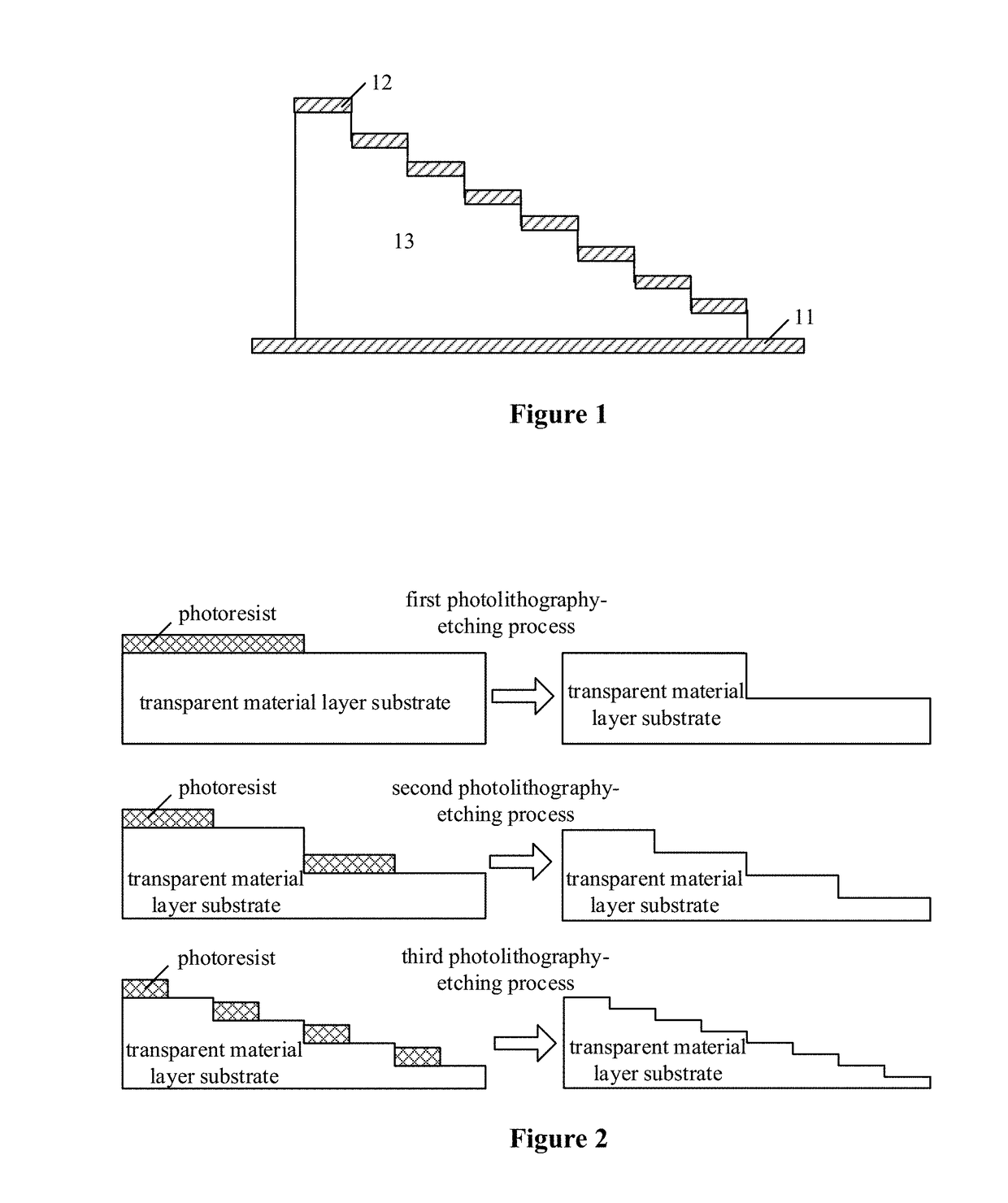
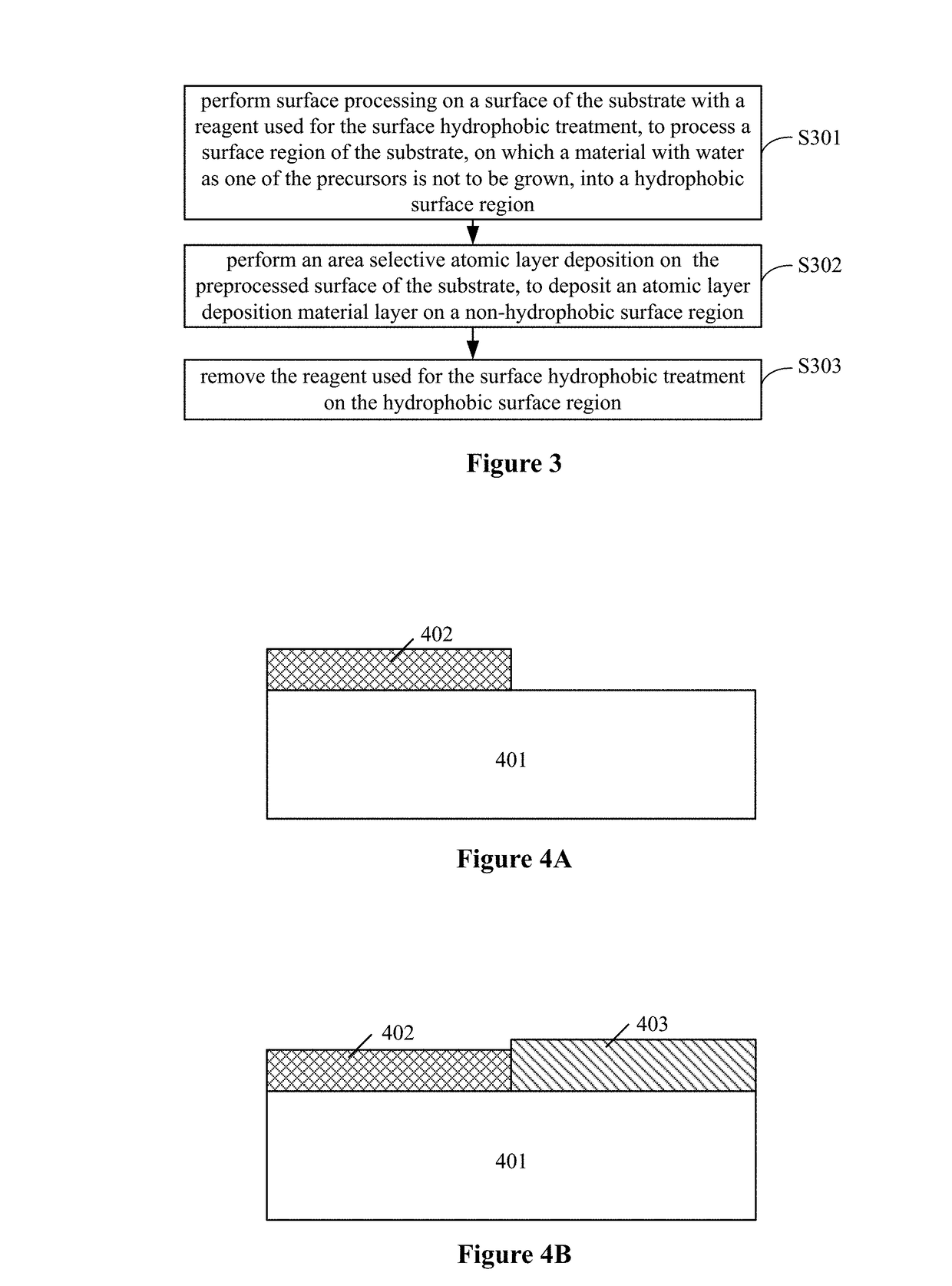
[0037]Before the embodiments according to the present disclosure are described, an area selective atomic layer deposition (Area Selective Atomic Layer Deposition, abbreviated as ASALD) process is introduced first.

[0038]The area selective atomic layer deposition process is a kind of atomic layer deposition process on selected surface where water is one of the precursors.

[0039]A material grown with water as one of the precursors generally grows well only on hydrophilic surfaces. In addition, the material grown with water as one of the precursors grows differently on different hydrophobic surfaces. The greater the hydrophobicity of a surface is, the higher the density of a hydrophobic material is, it is more difficult to grow the material with wate...


PUM


Abstract

A method for monolithic integration of a hyperspectral image sensor is provided, which includes: forming a bottom reflecting layer on a surface of the photosensitive region of a CMOS image sensor wafer; forming a transparent cavity layer composed of N step structures on the bottom reflecting layer through area selective atomic layer deposition processes, where N=2m, m≧1 and m is a positive integer; and forming a top reflecting layer on the transparent cavity layer. With the method, non-uniformity accumulation due to etching processes in conventional technology is minimized, and the cavity layer can be made of materials which cannot be etched. Mosaic cavity layers having such repeated structures with different heights can be formed by extending one-dimensional ASALD, such as extending in another dimension and forming repeated regions, which can be applied to snapshot hyperspectral image sensors, for example, pixels, and greatly improving performance thereof.

Description

CROSS-REFERENCE TO RELATED APPLICATION[0001]This application claims priority to Chinese Patent Application No. 201610214392.0, titled “METHOD OF MONOLITHIC INTEGRATION OF HYPERSPECTRAL IMAGE SENSOR,” filed with the State Intellectual Property Office of the People's Republic of China on Apr. 7, 2016, which is hereby incorporated by reference in its entirety.FIELD[0002]The present disclosure relates to the technical field of hyperspectral imaging, and in particular to a method for monolithic integration of a hyperspectral image sensor.BACKGROUND[0003]With help of hyperspectral imaging technology, a continuous spectrum can be divided into multiple spectral bands containing certain range of wavelengths, therefore, desired spectral bands can be further analyzed individually more in detail. Hence, hyperspectral imaging technology is widely applied to technical fields such as remote sensing, food science and bio-medical research. A previous hyperspectral imaging system is based on laborato...

Claims


Application Information

Patent Timeline
Patent Type & Authority Applications(United States)
IPC IPC(8): H01L27/146
CPCH01L27/14685H01L27/14629H01L27/14687H01L27/14621H01L27/14625H01L27/14632H01L31/02162H01L31/02327
Inventor CUI, HUSHANXIANG, JINJUANHE, XIAOBINYANG, TAOLI, JUNFENGZHAO, CHAO
Owner INST OF MICROELECTRONICS CHINESE ACAD OF SCI
Why Eureka
Try Eureka