ITO thin film sputtering process and ITO thin film sputtering device

A technology of sputtering process and sputtering equipment, which is applied in the field of ITO thin film sputtering process method and ITO thin film sputtering equipment, can solve the problems of increased cost, complicated equipment structure and operation, and reduced uniformity of TIO thin film to achieve uniformity Improve the uniformity of film deposition and reduce the effect of bombardment damage

Active Publication Date: 2014-07-23
BEIJING NAURA MICROELECTRONICS EQUIP CO LTD
View PDF5 Cites 4 Cited by
  • Summary
  • Abstract
  • Description
  • Claims
  • Application Information

AI Technical Summary

Problems solved by technology

However, adding a baffle mechanism will also reduce the uniformity of the TIO film, and the structure and operation of the equipment are complicated and the cost increases

Method used


Image

  • ITO thin film sputtering process and ITO thin film sputtering device
  • ITO thin film sputtering process and ITO thin film sputtering device
  • ITO thin film sputtering process and ITO thin film sputtering device

Examples


Embodiment Construction

[0041]Embodiments of the present invention are described in detail below, examples of which are shown in the drawings, wherein the same or similar reference numerals designate the same or similar elements or elements having the same or similar functions throughout. The embodiments described below by referring to the figures are exemplary and are intended to explain the present invention and should not be construed as limiting the present invention.

[0042] In describing the present invention, it should be understood that the terms "center", "longitudinal", "transverse", "length", "width", "thickness", "upper", "lower", "front", " Orientation or position indicated by "back", "left", "right", "vertical", "horizontal", "top", "bottom", "inner", "outer", "clockwise", "counterclockwise", etc. The relationship is based on the orientation or positional relationship shown in the drawings, and is only for the convenience of describing the present invention and simplifying the descript...


PUM


Abstract

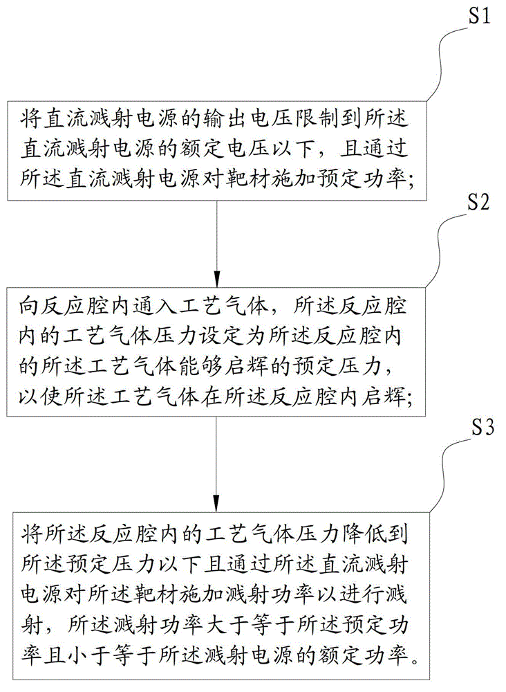
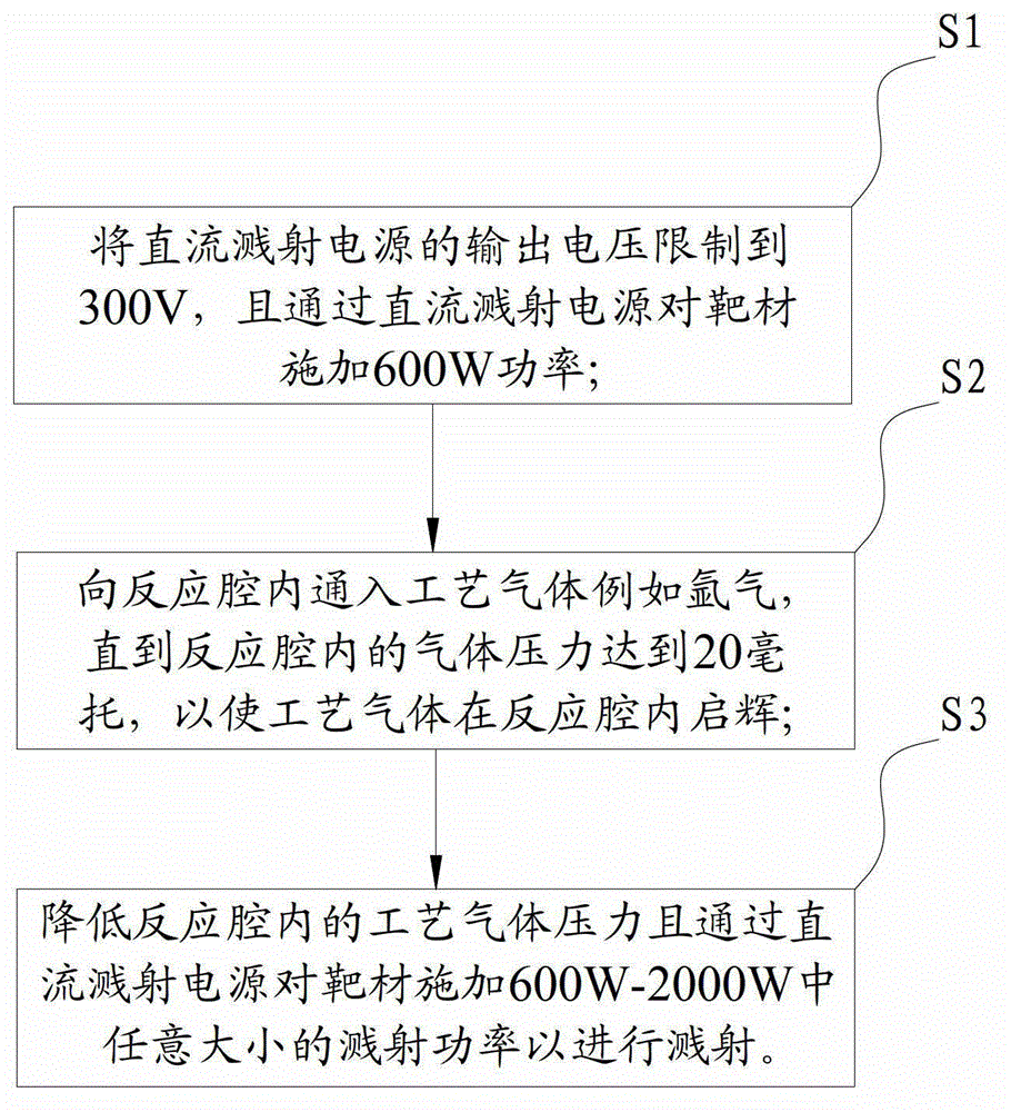
The invention discloses an ITO thin film sputtering process and an ITO thin film sputtering device. The ITO thin film sputtering process comprises steps of: 1) limiting the output voltage of a direct-current sputtering power supply to be lower than the nominal voltage of the direct-current sputtering power supply, and applying a preset power to a target material through the direct-current sputtering power supply; 2) feeding process gas into a reaction cavity, wherein the pressure of the process gas in the reaction cavity is set to be a preset pressure capable of glow starting of the process gas so that the process gas can be subjected to glow starting in the reaction cavity; and 3) lowering the pressure of the process gas in the reaction cavity to be lower than the preset pressure, applying a sputtering power to the target material through the direct-current sputtering power supply and sputtering, wherein the sputtering power is not less than the preset power and is not more than the rated power of the sputtering power supply. The ITO thin film sputtering process can lower the voltage peak value of glow starting.

Description

technical field [0001] The invention relates to the field of semiconductors, in particular to an ITO thin film sputtering process method and ITO thin film sputtering equipment. Background technique [0002] In recent years, due to the huge market demand for light-emitting diodes (LEDs), GaN-based LEDs have been widely used in different fields such as high-power lighting, automotive instrument displays, large-area outdoor displays, signal lights, and general lighting. [0003] In the LED chip manufacturing process, due to the low doping of P-type GaN and the low light transmittance of P-type ohmic metal contact, high contact resistance and low light transmittance will be caused, which seriously affects the improvement of the overall performance of the LED chip. In order to improve light extraction efficiency and reduce contact resistance, it is necessary to develop a transparent conductive film suitable for P-type GaN. As a transparent conductive film, ITO film (tin-doped in...

Claims


Application Information

Patent Timeline
Patent Type & Authority Applications(China)
IPC IPC(8): C23C14/34C23C14/35C23C14/08
CPCC23C14/086
Inventor 耿波叶华文利辉杨玉杰夏威王厚工丁培军
Owner BEIJING NAURA MICROELECTRONICS EQUIP CO LTD
Why Eureka
Try Eureka