
Light conversion device, preparation method thereof and infrared imaging device

A technology of optical conversion and devices, applied in the direction of electric solid-state devices, semiconductor devices, electrical components, etc., can solve the problems of difficult to achieve large-area replication, difficult to obtain gain, high process difficulty, etc., to meet portable imaging and realize large-scale The effect of low production and process difficulty

Inactive Publication Date: 2019-02-05
TCL CORPORATION
View PDF6 Cites 0 Cited by
  • Summary
  • Abstract
  • Description
  • Claims
  • Application Information

AI Technical Summary

Problems solved by technology

[0005] The object of the present invention is to provide a light conversion device and its preparation method, and infrared imaging equipment, aiming to solve the problems of high power consumption, poor portability, complex structure, high process difficulty, Problems of high production cost, difficulty in achieving large-area replication, and difficulty in obtaining high gain

Method used


Image

  • Light conversion device, preparation method thereof and infrared imaging device
  • Light conversion device, preparation method thereof and infrared imaging device
  • Light conversion device, preparation method thereof and infrared imaging device

Examples


Embodiment Construction

[0025] In order to make the object, technical solution and advantages of the present invention clearer, the present invention will be further described in detail below in conjunction with the accompanying drawings and embodiments. It should be understood that the specific embodiments described here are only used to explain the present invention, not to limit the present invention.

[0026] In the description of the present invention, it should be understood that the terms "first" and "second" are used for description purposes only, and cannot be interpreted as indicating or implying relative importance or implicitly indicating the quantity of indicated technical features. Thus, a feature defined as "first" and "second" may explicitly or implicitly include one or more of these features. In the description of the present invention, "plurality" means two or more, unless otherwise specifically defined.

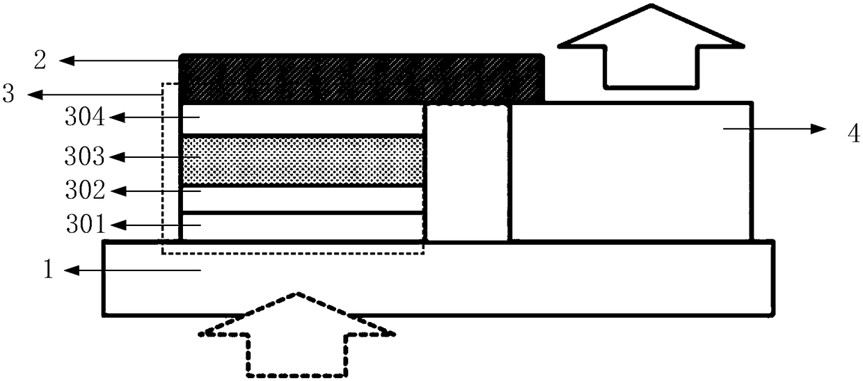
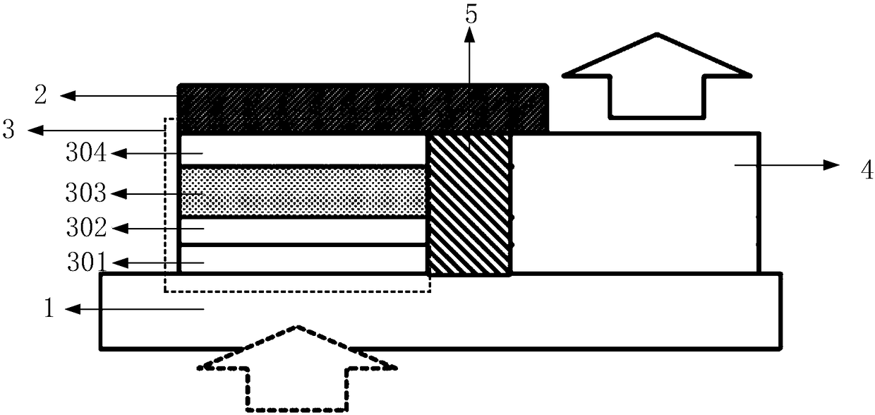
[0027] see figure 1 , figure 1 Schematic diagram of the structure of the l...


PUM


Abstract

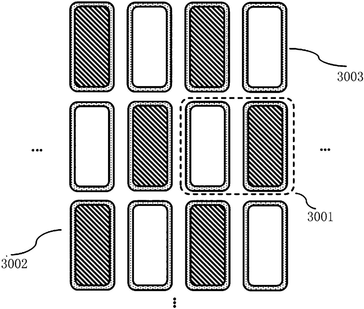
The invention belongs to the field of display devices, and provides a light conversion device, a preparation method thereof and an infrared imaging device. According to the light conversion device provided by the present invention, a photosensitive member and a light-emitting member are arranged side by side on a substrate, and the photosensitive member is set as a photoconductor structure provided with a second electrode, a first electron transport layer, a light absorbing layer, and a second electron transport layer which are laminated. The photoconductor structure replacing an existing diode structure has high light detection efficiency, so that the device has higher light guiding and light emitting efficiency. Due to the compact structure, small size and light weight of the device, therequirements for portable imaging of the device are met. And because each pixel has a simple structure and low process difficulty, each pixel is suitable for the existing printing preparation process, which can realize large-area copying and reduce production cost.

Description

technical field [0001] The invention belongs to the field of display devices, and in particular relates to a light conversion device, a preparation method thereof, and an infrared imaging device. Background technique [0002] Infrared imaging technology has been widely used in medical, military, night vision, satellite and civilian fields, and has always been a hot spot in scientific research. In recent decades, researchers have proposed imaging devices that can convert low-frequency infrared light to higher-frequency near-infrared or high-frequency visible light. [0003] The usual infrared-visible conversion imaging device (or photon energy up-conversion device) is a device based on silicon materials and photomultiplier tubes. The device is large in size. When it is used as a wearable night vision device, it has high power consumption and poor portability. Shortcomings. In order to improve the aforementioned shortcomings, researchers have turned to film-based night visio...

Claims


Application Information

Patent Timeline
Patent Type & Authority Applications(China)
IPC IPC(8): H01L27/28H01L27/30
CPCH10K65/00H10K39/32
Inventor 陈崧曹蔚然杨一行向超宇钱磊
Owner TCL CORPORATION
Learn More