OLED (organic light emitting diode) display substrate, manufacture method thereof and display device

A technology for display substrates and manufacturing methods, applied in the fields of final product manufacturing, sustainable manufacturing/processing, photovoltaic power generation, etc., can solve the problems of removing pixel defining layer materials and affecting the packaging effect of organic light-emitting display performance, etc., to achieve guaranteed performance, Guarantee the effect of encapsulation effect

Active Publication Date: 2019-02-19
BOE TECH GRP CO LTD
View PDF5 Cites 14 Cited by
  • Summary
  • Abstract
  • Description
  • Claims
  • Application Information

AI Technical Summary

Problems solved by technology

[0004] However, the existing undercut steps are generally formed before making the pixel definition layer. After the undercut steps are formed, when the pixel definition layer is subsequently prepared, the material of the pixel definition layer will be filled at the bottom of the undercut steps, and because the upper surface of the undercut steps It will block the exposure light, therefore, it is difficult to remove the pixel defining layer material at the bottom of the undercut step by exposure, so that when the cathode is subsequently deposited, the cathode cannot break at the edge of the upper surface of the undercut step, thereby affecting the actual packaging effect and organic light emission. Display performance

Method used


Image

  • OLED (organic light emitting diode) display substrate, manufacture method thereof and display device
  • OLED (organic light emitting diode) display substrate, manufacture method thereof and display device
  • OLED (organic light emitting diode) display substrate, manufacture method thereof and display device

Examples


Embodiment 1

[0089] Such as Figure 1-Figure 11 As shown, the manufacturing method of the OLED display substrate of this embodiment includes the following steps:

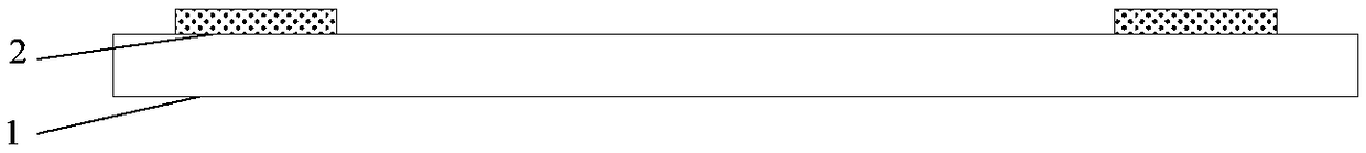
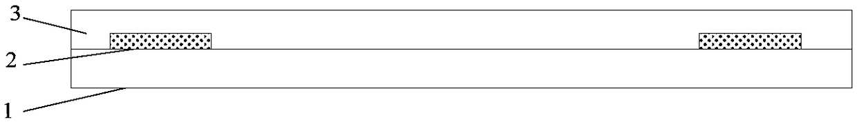
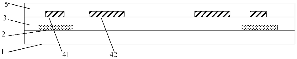
[0090] Step 1, such as figure 1 As shown, a base substrate 1 is provided, and an active layer 2 of a thin film transistor is formed on the base substrate 1;

[0091] Wherein, the base substrate 1 can be a rigid substrate or a flexible substrate, the rigid substrate includes a glass substrate and a quartz substrate, and the flexible substrate includes a PI (polyimide) substrate.

[0092] Specifically, a layer of semiconductor material is deposited on the base substrate 1, a layer of photoresist is coated on the semiconductor material, and a mask is used to expose the photoresist to form photoresist unretained regions and The photoresist completely reserved area, wherein, the photoresist completely reserved area corresponds to the area where the pattern of the active layer 2 is located, and the photoresist unreserved area corres...

Embodiment 2

[0120] The manufacturing method of the OLED display substrate of this embodiment includes the following steps:

[0121] Step 1. Provide a base substrate, and form a reflective pattern on the base substrate;

[0122] Wherein, the base substrate may be a rigid substrate or a flexible substrate, the rigid substrate includes a glass substrate and a quartz substrate, and the flexible substrate includes a PI (polyimide) substrate.

[0123] Specifically, sputtering or thermal evaporation can be used to deposit a thickness of about The metal layer, the metal layer can be Cu, Al, Ag, Mo, Cr, Nd, Ni, Mn, Ti, Ta, W and other metals and alloys of these metals, the metal layer can be a single-layer structure or a multi-layer structure, many Layer structure such as Cu\Mo, Ti\Al\Ti, Mo\Al\Mo, etc. A layer of photoresist is coated on the metal layer, and a mask is used to expose the photoresist, so that the photoresist forms a photoresist unreserved area and a photoresist reserved area, ...


PUM


Abstract

The invention provides an OLED (organic light emitting diode) display substrate, a manufacture method thereof and a display device, and belongs to the technical field of display. The manufacture method of the OLED display substrate includes the steps: forming an inverted table-shaped structure enclosing a cutting area on the periphery of the cutting area of the OLED display substrate; forming a reflective graphic between the inverted table-shaped structure and a base plate of the OLED display substrate before forming the inverted table-shaped structure. When a cathode of the OLED display substrate is formed, the edge of the cathode on the upper surface of the inverted table-shaped structure naturally fractures. The orthographic projection of the inverted table-shaped structure on the baseplate is positioned in the orthographic projection of the reflective graphic on the base plate. The packaging effect of the OLED display substrate can be ensured, and the performance of the display device is further ensured.

Description

technical field [0001] The invention relates to the field of display technology, in particular to an OLED display substrate, a manufacturing method thereof, and a display device. Background technique [0002] With the development of flexible display technology, flexible displays of different shapes become new requirements, and it is often necessary to cut the organic light emitting display to remove a part of the organic light emitting display. After cutting the organic light-emitting display, the edge of the cutting area is prone to infiltration of water and oxygen along the interlayer, resulting in poor display, especially the cathode of the organic light-emitting display is formed by evaporation on the entire surface. After cutting the organic light-emitting display, Since the side surface of the cathode is exposed, water and oxygen easily penetrate into the OLED display along the cathode. [0003] In order to solve the above problems, in the prior art, when making an or...

Claims


Application Information

Patent Timeline
Patent Type & Authority Applications(China)
IPC IPC(8): H01L27/32
CPCH10K59/12H10K59/1201Y02E10/549Y02P70/50H10K59/123H10K59/1213H10K59/131H10K50/856H10K71/851H10K77/10H10K59/122H10K71/00H10K2102/302
Inventor 王和金王品凡
Owner BOE TECH GRP CO LTD
Why Eureka
Try Eureka