Eureka AIR delivers breakthrough ideas for toughest innovation challenges, trusted by R&D personnel around the world.

GaN-based device for artificial photosynthesis and preparation method thereof

An artificial photosynthesis, gallium nitride-based technology, applied in the field of gallium nitride-based devices, can solve the problems of uneven electron collection and difficulty in improving cathode efficiency, and achieve high electron-hole separation efficiency, reduced emissions, and high absorption coefficient Effect

Active Publication Date: 2021-08-06
HEBEI UNIV OF TECH
View PDF0 Cites 0 Cited by
  • Summary
  • Abstract
  • Description
  • Claims
  • Application Information

AI Technical Summary

Problems solved by technology

And the small-area ohmic contact deposited on the surface of the anode makes the collection of electrons on the device uneven, and the electrons are transferred from the anode to the cathode, which makes it difficult to improve the efficiency of the cathode.

Method used


Image

  • GaN-based device for artificial photosynthesis and preparation method thereof

Examples


Embodiment Construction

[0016] The present invention will be further described below in conjunction with the accompanying drawings and specific embodiments.

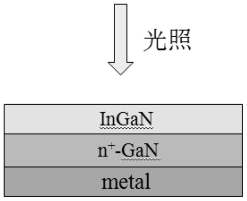
[0017] refer to figure 1 , the GaN-based device for artificial photosynthesis of the present invention has a metal substrate (Cu, In, Sn, Ag, Au, Pb, or Cd, etc.), n + - GaN layer, InGaN layer.

[0018] Its preparation method is as follows:

[0019] 1) On the clean n-type heavily doped gallium nitride layer, the InGaN epitaxial layer is grown by molecular beam epitaxy to obtain n + -GaN / InGaN structure;

[0020] 2) the above n by a bonding machine + -GaN / InGaN structures bonded on metal substrates, either using flip-chip technology or using conductive adhesives to obtain n + -GaN / InGaN structure bonded to the metal substrate, making n + -GaN is in contact with metal and the contact resistance of the contact interface is less than 1x10 -4 Ωcm 2 ; Get device. Excessive contact resistance is not conducive to the transport of holes and ele...


PUM

PropertyMeasurementUnit
energy conversion efficiencyaaaaaaaaaa

Abstract

The invention discloses a GaN-based device for artificial photosynthesis, with a metal substrate (Cu, In, Sn, Ag, Au, Pb, Cd, etc.), n + ‑GaN, InGaN layer, the preparation steps are as follows: use molecular beam epitaxy to grow an InGaN layer on the n-type heavily doped GaN layer, and then use physical or chemical methods (such as bonding, flip-chip bonding, etc.) to obtain the GaN-based epitaxial wafer , conductive glue, etc.) and the metal substrate are bonded together, so that the electrons in the GaN-based battery can be smoothly introduced to the metal substrate, and a gallium nitride device for artificial photosynthesis is obtained. The gallium nitride device of the present invention has the advantages of high absorption coefficient, high electron-hole separation efficiency, and good current uniformity, and can be used as a photoanode material in artificial photosynthesis, and is very useful for reducing carbon dioxide emissions and developing and utilizing new energy sources. important meaning.

Description

technical field [0001] The invention relates to a gallium nitride-based device, in particular to a gallium nitride-based device for artificial photosynthesis and a preparation method thereof. Background technique [0002] With the rapid development of the economy, a large amount of non-renewable resources such as coal and oil are burned. While consuming these fossil fuels, it also aggravates the deterioration of the environment, the most important of which is the greenhouse effect, which causes global warming and sea level rise. , Increase in pests and diseases and other environmental problems. [0003] It is well known that plants and certain bacteria can convert atmospheric CO 2 fixed, the CO 2 Transform into organic matter with industrial value and release oxygen. As early as the 1990s, some researchers proposed the concept of artificial photosynthesis. Using artificial photosynthesis technology can not only photolyze water, but also convert CO 2 Reduction to HCOOH, ...

Claims


Application Information

Patent Timeline
Patent Type & Authority Patents(China)
IPC IPC(8): H01G9/20H01G9/00
CPCH01G9/0029H01G9/205Y02E10/542
Inventor 陈贵锋刘巍马苗苗张辉解新建李媛陶俊光刘国栋
Owner HEBEI UNIV OF TECH
Why Eureka
Eureka Blog
Learn More