Band gap tunable copper zinc tin sulfur semiconductor film and preparation method thereof

A copper-zinc-tin-sulfur and semiconductor technology, which is applied in the field of adjustable band gap copper-zinc-tin-sulfur semiconductor films and their preparation, can solve the problem that the crystal quality and structural properties of the films cannot be optimized, and it is difficult to obtain high-quality copper-zinc-tin-sulfur films. It can improve the photoelectric conversion efficiency, reduce the infiltration of harmful gases, and achieve good compactness.

Inactive Publication Date: 2012-07-11
WUYI UNIV
View PDF5 Cites 13 Cited by
  • Summary
  • Abstract
  • Description
  • Claims
  • Application Information

AI Technical Summary

Problems solved by technology

However, this method cannot adjust the order of metal evaporation, and cannot perform two or three evaporations on one of zinc, tin, and copper to optimize the crystalline quality and structural properties of the film, and there are also insufficient vulcanization of the precursor film, which is difficult. Obtain high-quality copper-zinc-tin-sulfur films with controlled gap
Copper-zinc-tin-sulfur thin films are multi-component compounds, and their photoelectric properties are very sensitive to structural defects caused by improper atomic ratio and lattice matching, and greatly affect the improvement of their efficiency.

Method used


Image

  • Band gap tunable copper zinc tin sulfur semiconductor film and preparation method thereof
  • Band gap tunable copper zinc tin sulfur semiconductor film and preparation method thereof

Examples


preparation example Construction

[0031] A preparation process for an adjustable bandgap copper-zinc-tin-sulfur semiconductor thin film, the process is as follows:

[0032] 1) Clean the substrate substrate

[0033] Using a glass slide as the substrate, first use ammonia water (the ammonia content is 27wt%), 30wt% hydrogen peroxide solution and water at a volume ratio of 0.5:1:5, and then ultrasonically clean the No. 1 cleaning solution obtained after mixing Clean for 5 minutes, then wash with deionized water for 3 times, then use the volume ratio of 36.5wt% hydrochloric acid, 30wt% hydrogen peroxide solution and water to mix the obtained No. 2 cleaning solution for ultrasonic cleaning for 5 minutes, Then wash 3 times with deionized water, and store the cleaned slides in 75% alcohol solution for later use.

[0034] 2) Preparation of layered metal thin film precursor

[0035] Put 99.99% and above purity powder or flake or wire copper, zinc and tin metals in different tungsten boats, and conduct thermal evapora...

Embodiment 1

[0039] Example 1 (Cu 2.1 Zn 1.05 SnS 4 )

[0040] Take copper powder (10.9mg), zinc powder (5.5mg) and tin powder (9.6mg) and place them in three tungsten boats respectively, and conduct thermal evaporation deposition of the metal layer on a vacuum coating machine. The order of evaporation deposition is Cu-Zn- Sn metal layer, to obtain a layered metal thin film precursor deposited on a glass slide.

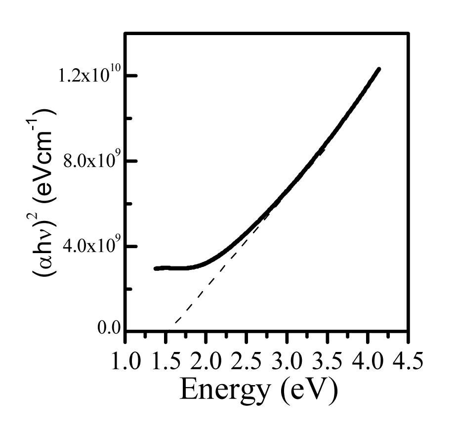
[0041] Put the above glass slide and sufficient amount of sulfur powder in a vacuum furnace to heat, first raise the temperature to 400 °C for 60 min, then keep it warm for 2 h, and finally obtain a copper-zinc-tin with a thickness of 1 μm and an optical band gap of 1.51 eV. Sulfur semiconductor thin films.

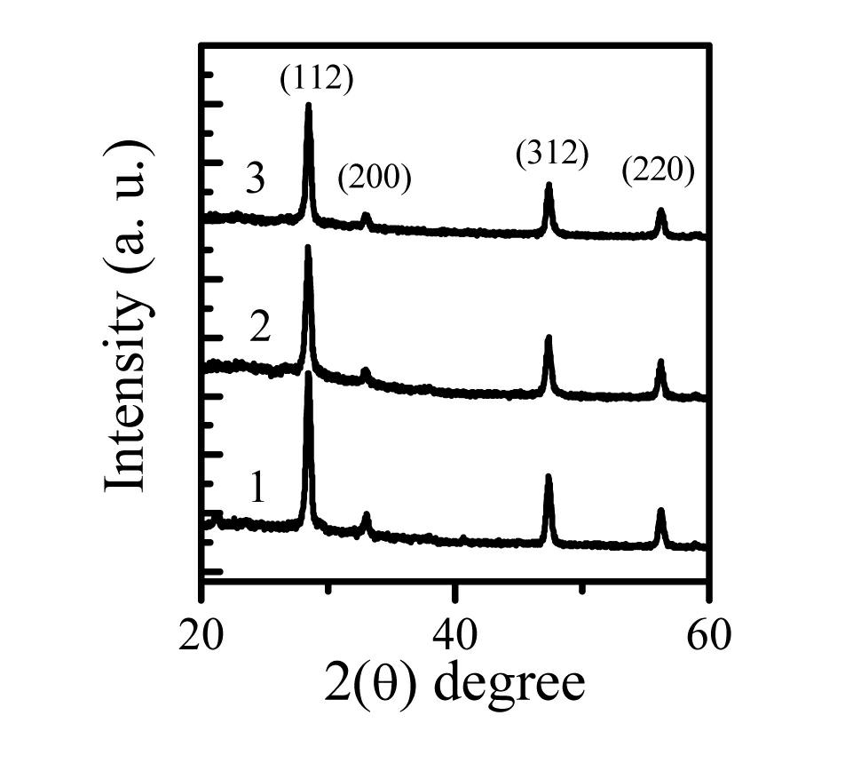
[0042] figure 1It is the XRD figure of embodiment 1 and comparative example semiconductor thin film, there are three curves in the figure, is respectively curve 3, curve 2, curve 1 from top to bottom, and curve 1 is the XRD figure of embodiment 1 semiconductor thin fil...

Embodiment 2

[0043] Example 2 (Cu 2.4 Zn 0.95 SnS 4 )

[0044] Take copper wire (12.1mg), zinc sheet (5.5mg) and tin wire (9.6mg) and place them in three tungsten boats, and conduct thermal evaporation deposition of metal layers on a vacuum coating machine. The order of evaporation deposition is Cu-Sn- The Zn metal layer was deposited on a glass slide to obtain a layered metal thin film precursor.

[0045] Put the above glass slide and sufficient amount of sulfur powder in a vacuum furnace to heat, first raise the temperature to 300 ℃ for 60 minutes, and then keep it warm for 2 hours, finally get the adjustable bandgap copper-zinc with a thickness of 1.1μm and an optical bandgap of 1.2eV Tin-sulfur semiconductor thin films.


PUM

PropertyMeasurementUnit
thicknessaaaaaaaaaa
optical band gapaaaaaaaaaa
thicknessaaaaaaaaaa

Abstract

The invention discloses a band gap tunable copper zinc tin sulfur semiconductor film and a preparation method thereof. The chemical formula of the semiconductor film is CuaZnbSncS4, wherein 1<= a<=3, 0.3<=b<= 2, 0.2<=c<=2. The preparation method comprises the steps of adding high purity metals of copper, zinc and tin to different tungsten boats and molybdenum boat, acquiring a lamellar metal film precursor through vacuum thermal evaporation, and vulcanizing the precursor in vacuum to obtain the band gap tunable copper zinc tin sulfur semiconductor film. Adjustments of components and optical properties are achieved and high-quality copper zinc tin sulfur semiconductor film is obtained by changes of evaporation order, mass ratio or mole ratio. The chemical formula of the semiconductor film has the advantages of being simple in device requirements, low in cost, environment friendly and pollution-free, suitable for industrial production and capable of being produced in a large scale and controlling band gaps.

Description

technical field [0001] The invention belongs to the technical field of photoelectric materials, and relates to an adjustable bandgap copper-zinc-tin-sulfur semiconductor film and a preparation method thereof. Background technique [0002] With the depletion of non-renewable resources such as coal, oil and natural gas and the intensification of environmental pollution, human beings are turning their attention to new energy, especially renewable new energy. As a renewable resource, solar energy will not change the earth's thermal balance and ecosystem. It has the characteristics of inexhaustible, safe to use, extensive and sufficient resources, long life and maintenance-free. In the effective use of solar energy, photovoltaic power generation is the fastest growing and most dynamic research field in recent years, and has received attention and strong support from governments around the world. The large-scale utilization of solar energy is mainly faced with the challenges of i...

Claims


Application Information

Patent Timeline
Patent Type & Authority Applications(China)
IPC IPC(8): H01L31/032H01L31/18C23C14/24C23C14/58C23C14/06
CPCY02P70/50
Inventor 范东华彭辉仁
Owner WUYI UNIV
Why Eureka
Try Eureka